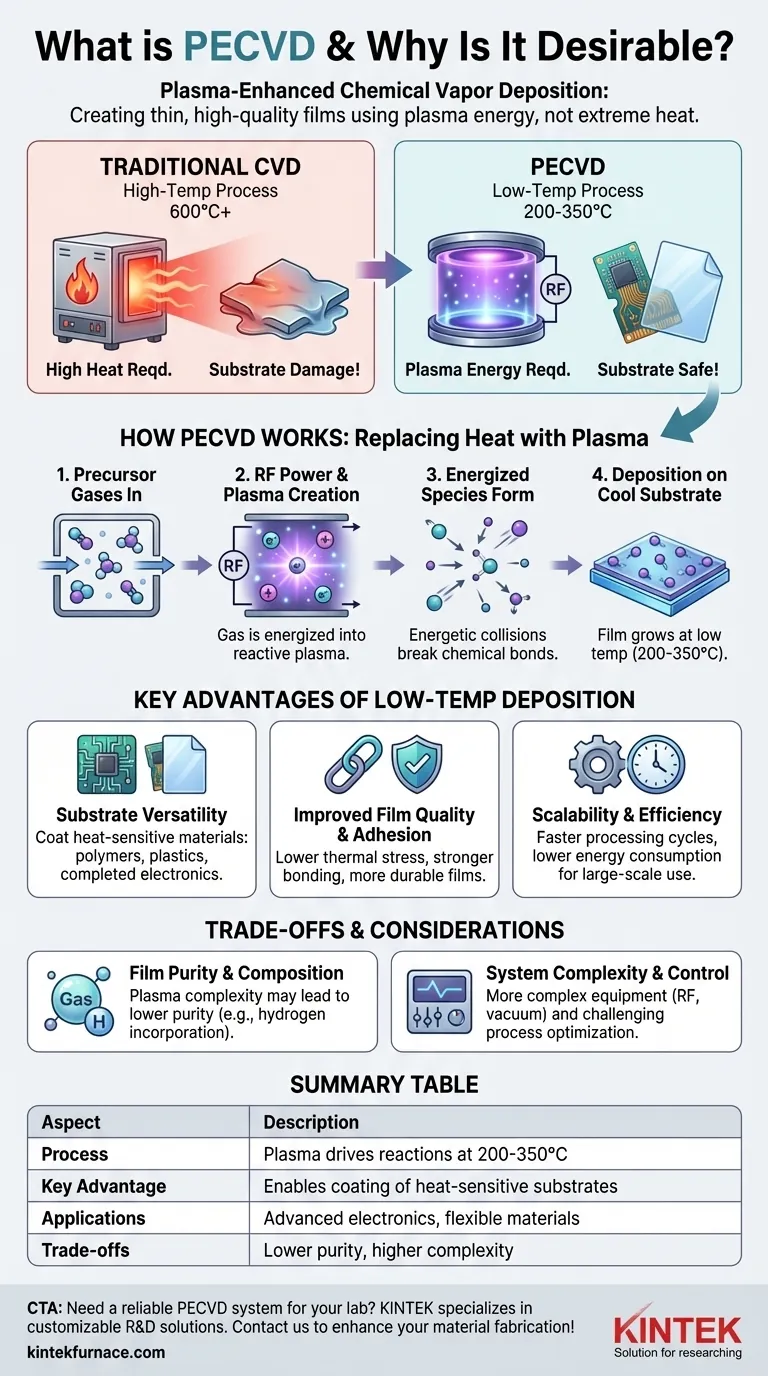
In short, Plasma-Enhanced Chemical Vapor Deposition (PECVD) is a process for creating exceptionally thin, high-quality films on a surface. It uses an energized gas, or plasma, to drive the chemical reactions needed for deposition. The defining advantage of this method is that it works at significantly lower temperatures than traditional Chemical Vapor Deposition (CVD), making it essential for modern manufacturing.
The fundamental value of PECVD lies in its ability to deposit high-performance films on substrates that cannot survive extreme heat. By replacing intense thermal energy with plasma energy, it unlocks the fabrication of advanced electronics and materials on heat-sensitive components that would otherwise be damaged or destroyed.
How PECVD Works: Replacing Heat with Plasma
To understand why PECVD is so impactful, we first need to look at the limitations of its predecessor, conventional CVD.
The Traditional CVD Challenge: High Temperatures
Traditional CVD works by heating a substrate to very high temperatures (often over 600°C). Precursor gases are then introduced, and the intense heat provides the energy needed to break them down and react, depositing a solid film onto the hot surface.
This high thermal budget is a major constraint. It prohibits the use of substrates that would melt, deform, or degrade, such as plastics or complex semiconductor wafers that already contain sensitive circuitry.
The Plasma Solution: An Energized State of Matter
PECVD overcomes this heat barrier by using plasma. A plasma is created by applying a strong electric field (typically Radio Frequency or RF) to a low-pressure gas inside the reaction chamber.
This field energizes the gas, stripping electrons from their atoms and creating a highly reactive environment filled with ions, radicals, and free electrons. This is often called the fourth state of matter.
Driving the Reaction Without Intense Heat
In a PECVD process, the energetic electrons within the plasma collide with the precursor gas molecules. These collisions transfer enough energy to break the chemical bonds of the precursor molecules, creating the reactive species needed for deposition.
Crucially, this happens while the substrate itself remains at a much lower temperature, typically in the range of 200°C to 350°C, and sometimes even at room temperature. The energy for the reaction comes from the plasma, not from heating the substrate.
Deposition and Film Growth
The reactive chemical fragments then travel to the surface of the relatively cool substrate. There, they settle and bond, gradually building a uniform, dense, and high-quality thin film.
Key Advantages of Low-Temperature Deposition
The ability to operate at low temperatures is not just a minor improvement; it fundamentally changes what is possible in materials science and manufacturing.
Substrate Versatility
Because high heat is no longer a requirement, PECVD can be used to coat a vast range of materials. This includes polymers, flexible plastics, and fully fabricated semiconductor devices that cannot tolerate another high-temperature processing step.
Improved Film Quality and Adhesion
High temperatures can create significant thermal stress between the deposited film and the substrate, leading to cracking, peeling, or poor adhesion.
PECVD's low-temperature nature minimizes this stress, resulting in stronger bonding and more durable, reliable films.
Scalability and Efficiency
In a manufacturing environment, lower operating temperatures translate to faster processing cycles, as less time is spent on heating and cooling. This also reduces overall energy consumption, making the process more cost-effective and suitable for large-scale production.
Understanding the Trade-offs and Considerations
While powerful, PECVD is not a universal solution. An objective assessment requires acknowledging its trade-offs compared to purely thermal methods like Low-Pressure CVD (LPCVD).
Film Purity and Composition
The plasma environment is chemically complex. During deposition, atoms from the plasma gas (like hydrogen) can become incorporated into the growing film, affecting its purity and properties. For applications demanding the absolute highest purity, a high-temperature thermal process might be more suitable.
System Complexity and Cost
A PECVD reactor is inherently more complex than a simple thermal CVD furnace. It requires sophisticated RF power generators, electrode designs, and vacuum systems to control the plasma. This can increase the initial equipment cost and maintenance requirements.
Process Control
The introduction of plasma adds several variables to the process, including RF power, frequency, and gas pressure. While this offers more control over film properties, it also makes optimizing the process more challenging than simply tuning temperature and pressure in a thermal system.
Making the Right Choice for Your Goal
Selecting the correct deposition technology depends entirely on the requirements of your substrate and the desired properties of the final film.
- If your primary focus is depositing on heat-sensitive substrates: PECVD is the definitive choice due to its low-temperature operation, enabling fabrication on polymers, plastics, and completed integrated circuits.
- If your primary focus is achieving maximum film purity on a thermally stable substrate: A traditional high-temperature process like LPCVD may be preferred to avoid potential impurities from the plasma.
- If your primary focus is balancing performance, versatility, and manufacturing cost: PECVD offers a powerful and widely adopted solution that delivers high-quality films across a vast range of materials and applications.
Ultimately, understanding the interplay between thermal and plasma energy empowers you to select the most effective tool for your material fabrication goals.
Summary Table:
| Aspect | Description |
|---|---|
| Process | Uses plasma to drive chemical reactions for deposition at lower temperatures (200°C-350°C) |
| Key Advantage | Enables coating of heat-sensitive substrates like plastics and semiconductors without damage |
| Applications | Advanced electronics, flexible materials, and integrated circuits |
| Trade-offs | Potential for lower film purity and higher system complexity compared to thermal CVD |
Need a reliable PECVD system for your lab? KINTEK specializes in advanced high-temperature furnace solutions, including CVD/PECVD Systems, with deep customization to meet your unique experimental needs. Our expertise in R&D and in-house manufacturing ensures precise, efficient results for diverse laboratories. Contact us today to discuss how we can enhance your material fabrication processes!
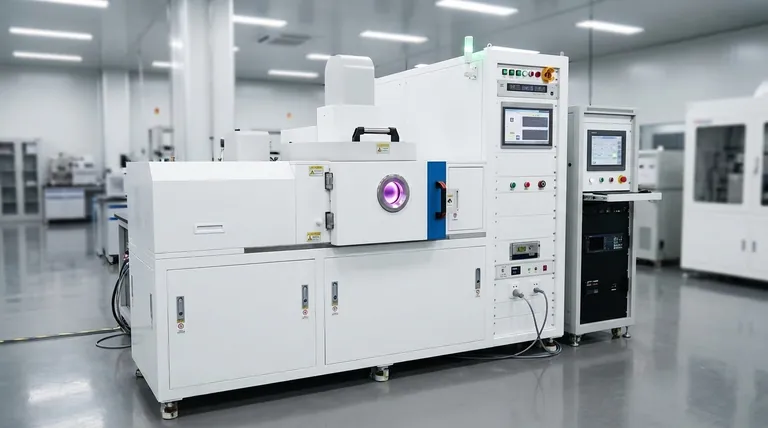
Visual Guide
Related Products
- RF PECVD System Radio Frequency Plasma Enhanced Chemical Vapor Deposition
- Slide PECVD Tube Furnace with Liquid Gasifier PECVD Machine
- Inclined Rotary Plasma Enhanced Chemical Deposition PECVD Tube Furnace Machine
- Inclined Rotary Plasma Enhanced Chemical Deposition PECVD Tube Furnace Machine
- 915MHz MPCVD Diamond Machine Microwave Plasma Chemical Vapor Deposition System Reactor
People Also Ask
- What is PECVD specification? A Guide to Choosing the Right System for Your Lab
- How is silicon dioxide deposited from tetraethylorthosilicate (TEOS) in PECVD? Achieve Low-Temperature, High-Quality SiO2 Films
- What is the role of RF power in PECVD and how does the RF-PECVD process work? Master Thin Film Deposition Control
- What is RF in PECVD? A Critical Control for Plasma Deposition
- What are the key advantages of PECVD technology? Achieve Low-Temperature, High-Quality Thin Film Deposition


