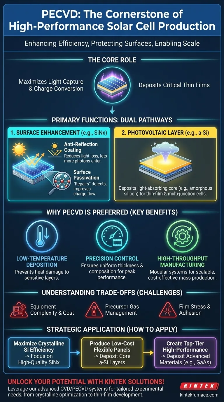
In short, Plasma Enhanced Chemical Vapor Deposition (PECVD) is a cornerstone technology used to deposit critical thin films onto solar cells. These films serve two primary purposes: enhancing the cell's efficiency by improving light absorption and charge carrier movement, and protecting the cell's delicate surfaces. Without PECVD, manufacturing high-performance, cost-effective solar panels at scale would not be possible.
The core role of PECVD is not simply to add a layer, but to fundamentally improve a solar cell's performance. It achieves this by depositing highly controlled films that both maximize the light captured and optimize how that light energy is converted into electrical current within the cell.
The Two Primary Functions of PECVD
PECVD is not a single-purpose tool; it's a versatile process used to create different types of layers, each with a distinct and vital function. These can be broadly categorized into surface enhancement and the creation of the core photovoltaic material itself.
Function 1: Surface Anti-Reflection and Passivation
For most conventional crystalline silicon solar cells, the most important application of PECVD is depositing a thin film of silicon nitride (SiNx). This single layer performs two jobs simultaneously.
First, it acts as an anti-reflective coating. The silicon surface is naturally shiny and reflects a significant portion of incoming sunlight. The precisely engineered SiNx layer reduces this reflection, allowing more photons to enter the cell and generate power.
Second, the film provides surface passivation. The silicon crystal structure has microscopic imperfections and "dangling bonds" at its surface, which can trap charge carriers (electrons) and reduce the cell's efficiency. The hydrogen-rich SiNx film deposited by PECVD effectively "repairs" these defects, allowing charge carriers to move freely and contribute to the electrical current.
Function 2: Depositing the Photovoltaic Layer Itself
In other types of solar cells, particularly thin-film solar cells, PECVD is used to deposit the primary light-absorbing layer. This is the material that actually converts photons into electron-hole pairs.
Materials like amorphous silicon (a-Si) are deposited using PECVD to create the core of the solar cell. This technique is also instrumental in the production of high-efficiency, multi-junction cells using materials like gallium arsenide (GaAs), which are common in space applications where performance is paramount.
Why PECVD is the Preferred Method
Other deposition methods exist, but PECVD offers a unique combination of benefits that make it ideal for the delicate and precise demands of solar cell manufacturing.
The Advantage of Low-Temperature Deposition
The "Plasma Enhanced" aspect of PECVD is its key advantage. The plasma provides the energy needed to drive the chemical reactions for deposition, rather than relying solely on high heat.
This allows the process to run at significantly lower temperatures compared to traditional Chemical Vapor Deposition (CVD). This is critical for preventing damage to the underlying layers of the solar cell, which can be sensitive to thermal stress.
Precision Control Over Film Quality
PECVD systems provide exceptionally precise control over film thickness, chemical composition, and uniformity across the entire substrate.
This level of control is directly linked to the final performance of the solar cell. A uniform anti-reflective coating absorbs light evenly, and a well-composed passivation layer maximizes efficiency gains.
Designed for High-Throughput Manufacturing
Modern PECVD equipment is modular and designed for mass production. It enables high throughput, high uptime, and efficient use of raw materials (precursor gases). These factors are essential for reducing the overall cost per watt of solar energy, making it more competitive.
Understanding the Trade-offs
While powerful, PECVD is a sophisticated process with its own set of challenges that engineers must manage.
Equipment Complexity and Cost
PECVD reactors are complex and represent a significant capital investment. They require careful maintenance and skilled operators to ensure consistent, high-quality results in a production environment.
Precursor Gas Management
The process relies on a steady and precise supply of precursor gases, some of which can be hazardous. Managing the storage, delivery, and handling of these materials is a critical safety and operational consideration.
Film Stress and Adhesion
Achieving the perfect film requires tuning numerous process parameters, including temperature, pressure, gas flow rates, and plasma power. Incorrect parameters can lead to high internal stress in the deposited film, causing it to crack or peel off the substrate, which ruins the cell.
How to Apply This to Your Goal
Your manufacturing strategy will dictate how you leverage PECVD technology.
- If your primary focus is maximizing the efficiency of standard crystalline silicon cells: Your key leverage point is optimizing the deposition of high-quality SiNx for superior anti-reflection and passivation.
- If your primary focus is producing low-cost, flexible thin-film panels: PECVD is the engine for depositing the core amorphous silicon (a-Si) or other photovoltaic layers at scale.
- If your primary focus is creating top-tier, high-performance cells for aerospace or concentrator systems: You will use PECVD to deposit advanced, high-purity materials like GaAs in complex multi-junction structures.
Ultimately, mastering PECVD is fundamental to advancing the cost-effectiveness and performance of photovoltaic technology.
Summary Table:
| Function | Key Applications | Benefits |
|---|---|---|
| Surface Anti-Reflection & Passivation | Deposits silicon nitride (SiNx) for reduced reflection and defect repair | Improves light absorption and charge carrier movement, increasing efficiency |
| Photovoltaic Layer Deposition | Creates core layers in thin-film cells (e.g., amorphous silicon, GaAs) | Enables high-performance, flexible, and multi-junction solar cells |
| Low-Temperature Processing | Uses plasma energy instead of high heat | Prevents damage to sensitive substrates, ideal for delicate solar cell structures |
| High-Throughput Manufacturing | Modular systems for mass production | Reduces costs, ensures uniformity, and supports scalable solar panel output |
Unlock the full potential of your solar cell production with KINTEK's advanced PECVD solutions! Leveraging exceptional R&D and in-house manufacturing, we provide diverse laboratories with tailored high-temperature furnace systems, including CVD/PECVD Systems, to precisely meet your unique experimental needs. Whether you're optimizing crystalline silicon cells or developing thin-film technologies, our deep customization capabilities ensure superior efficiency and cost-effectiveness. Contact us today to discuss how our expertise can elevate your photovoltaic innovations!
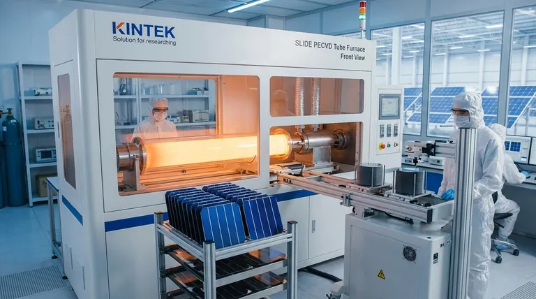
Visual Guide
Related Products
- Slide PECVD Tube Furnace with Liquid Gasifier PECVD Machine
- RF PECVD System Radio Frequency Plasma Enhanced Chemical Vapor Deposition
- Inclined Rotary Plasma Enhanced Chemical Deposition PECVD Tube Furnace Machine
- Inclined Rotary Plasma Enhanced Chemical Deposition PECVD Tube Furnace Machine
- Multi Heating Zones CVD Tube Furnace Machine for Chemical Vapor Deposition Equipment
People Also Ask
- What are the typical conditions for plasma-enhanced CVD processes? Achieve Low-Temperature Thin Film Deposition
- How does PECVD equipment contribute to TOPCon bottom cells? Mastering Hydrogenation for Maximum Solar Efficiency
- In which industries is the tube furnace commonly used? Essential for Materials Science, Energy, and More
- What role does a Tube Furnace play in the CVD growth of carbon nanotubes? Achieve High-Purity CNT Synthesis
- How does a hydrogen reduction environment in an industrial tube furnace facilitate gold-copper alloy microspheres?


