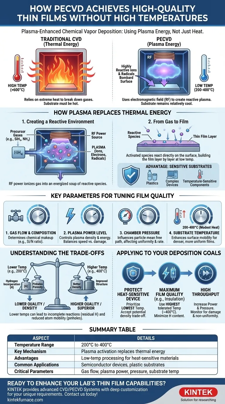
At its core, Plasma-Enhanced Chemical Vapor Deposition (PECVD) achieves high-quality thin films without extreme heat by using plasma to supply the necessary activation energy. Instead of relying on high temperatures to break down precursor gases, PECVD uses an electromagnetic field (typically radio frequency) to ionize the gas, creating a plasma filled with highly reactive ions and radicals that deposit onto the substrate at much lower temperatures, often between 200°C and 400°C.
The fundamental difference is the energy source. Traditional Chemical Vapor Deposition (CVD) uses thermal energy, heating the substrate to drive chemical reactions. PECVD uses the energetic particles within a plasma to do the same work, allowing the substrate itself to remain relatively cool.
How Plasma Replaces Thermal Energy
The genius of PECVD lies in its ability to separate the energy required for the chemical reaction from the temperature of the substrate.
Creating a Reactive Environment
In a PECVD chamber, precursor gases are introduced at low pressure. An RF power source is then applied, which strips electrons from the gas molecules.
This process creates a plasma—an energized soup of ions, electrons, free radicals, and neutral molecules. These free radicals are chemically unstable and extremely reactive.
From Gas to Film
These highly reactive species bombard the surface of the wafer or substrate. Because they are already in an activated state, they don't need high thermal energy from the substrate to react and form the desired thin film.
The chemical reactions happen directly on the surface as these particles arrive, building the film layer by layer.
The Advantage for Sensitive Substrates
This low-temperature capability is the primary reason PECVD is so valuable. It allows for deposition on materials that cannot withstand high heat, such as plastics, or on complex semiconductor devices that have already undergone previous processing steps with temperature-sensitive components.
Key Parameters for Tuning Film Quality
While plasma does the heavy lifting, the final quality of the film is not automatic. It depends on a careful balance of several critical process parameters.
Gas Flow and Composition
The specific precursor gases and their flow rates directly determine the chemical makeup and stoichiometry of the final film. For example, depositing silicon nitride (Si₃N₄) involves precise control of silane (SiH₄) and ammonia (NH₃) or nitrogen (N₂) gas flows.
Plasma Power Level
The amount of RF power applied controls the density and energy of the plasma. Higher power increases the deposition rate but can also lead to film damage from high-energy ion bombardment. It's a critical parameter for balancing speed and quality.
Chamber Pressure
Pressure influences the "mean free path" of particles, or how far they travel before colliding. Lower pressures can improve film uniformity across the wafer, while higher pressures can increase the deposition rate.
Substrate Temperature
Even in a "low-temperature" process, the substrate is still heated, typically to between 200°C and 400°C. This modest heat enhances the surface mobility of deposited atoms, helping them find stable positions and resulting in a denser, more uniform film with fewer defects.
Understanding the Trade-offs of Low-Temperature Deposition
PECVD is a powerful tool, but its low-temperature nature introduces specific compromises that must be managed.
The "Quality" Spectrum
While PECVD films are considered high-quality, films deposited at the higher end of the PECVD temperature range (350-400°C) are generally superior. They have better density and structure compared to those deposited at 200°C.
Hydrogen Incorporation
PECVD precursor gases are often hydrogen-based (e.g., silane). At lower temperatures, reactions may be incomplete, leaving hydrogen atoms incorporated into the film. This residual hydrogen can negatively impact the film's electrical properties and stability. Higher temperatures help drive off more hydrogen.
Film Density and Pinholes
Lower substrate temperatures reduce the surface mobility of the depositing atoms. This can prevent them from settling into the most stable, dense configuration, potentially leading to porous films or the formation of microscopic "pinholes," which can compromise the film's integrity.
Applying This to Your Deposition Goals
Your optimal PECVD process depends entirely on what you are trying to achieve.
- If your primary focus is protecting a heat-sensitive device: Prioritize the lowest possible deposition temperature your process will allow, and accept a potential trade-off in film density.
- If your primary focus is maximum film quality (e.g., electrical insulation): Use the highest temperature your substrate can tolerate (up to ~400°C) to minimize hydrogen content and maximize film density.
- If your primary focus is high throughput: You may increase plasma power and pressure to boost the deposition rate, but you must monitor for potential film damage and non-uniformity.
By understanding how plasma substitutes for heat, you can manipulate the key process levers to achieve the specific film properties your application demands.
Summary Table:
| Aspect | Details |
|---|---|
| Temperature Range | 200°C to 400°C |
| Key Mechanism | Plasma activation replaces thermal energy |
| Advantages | Low-temperature processing, suitable for heat-sensitive materials |
| Common Applications | Semiconductor devices, plastic substrates |
| Critical Parameters | Gas flow, plasma power, chamber pressure, substrate temperature |
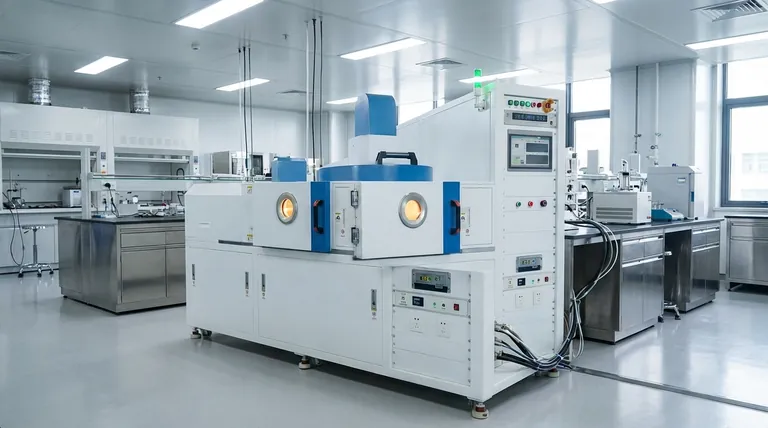
Ready to enhance your lab's thin film capabilities with tailored PECVD solutions? Leveraging exceptional R&D and in-house manufacturing, KINTEK provides diverse laboratories with advanced high-temperature furnace solutions. Our product line, including Muffle, Tube, Rotary Furnaces, Vacuum & Atmosphere Furnaces, and CVD/PECVD Systems, is complemented by our strong deep customization capability to precisely meet unique experimental requirements. Whether you're working with sensitive substrates or need high-quality film deposition, we can help optimize your process. Contact us today to discuss how our expertise can benefit your specific needs!
Visual Guide
Related Products
- RF PECVD System Radio Frequency Plasma Enhanced Chemical Vapor Deposition
- Slide PECVD Tube Furnace with Liquid Gasifier PECVD Machine
- Inclined Rotary Plasma Enhanced Chemical Deposition PECVD Tube Furnace Machine
- Inclined Rotary Plasma Enhanced Chemical Deposition PECVD Tube Furnace Machine
- Cylindrical Resonator MPCVD Machine System for Lab Diamond Growth
People Also Ask
- How are deposition rates and film properties controlled in PECVD? Master Key Parameters for Optimal Thin Films
- How is silicon dioxide deposited from tetraethylorthosilicate (TEOS) in PECVD? Achieve Low-Temperature, High-Quality SiO2 Films
- What are the advantages of PECVD in film deposition? Achieve Low-Temp, High-Quality Coatings
- What are the key advantages of PECVD technology? Achieve Low-Temperature, High-Quality Thin Film Deposition
- What are some promising applications of PECVD-prepared 2D materials? Unlock Advanced Sensing and Optoelectronics


