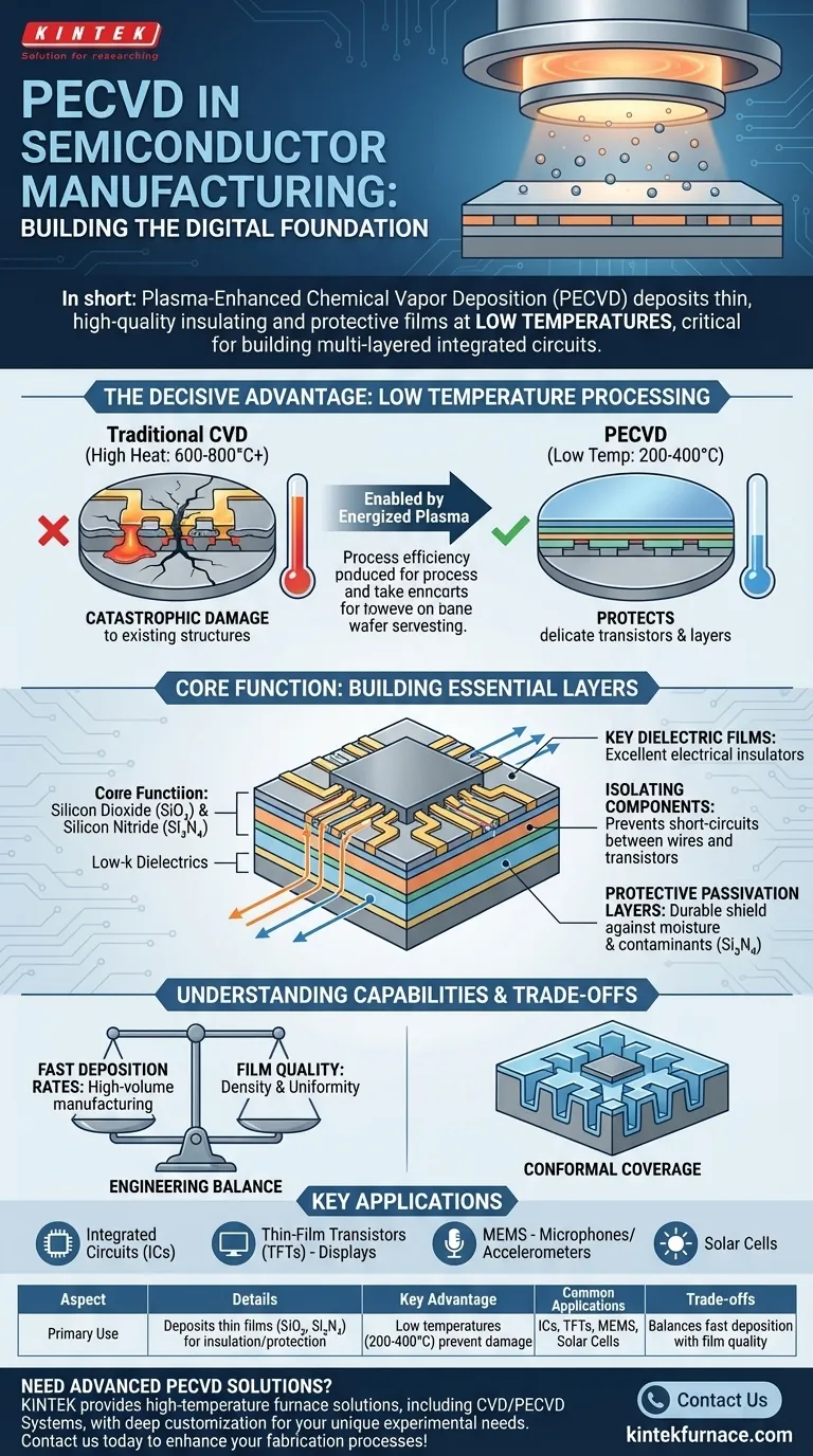
In short, Plasma-Enhanced Chemical Vapor Deposition (PECVD) is a cornerstone process in semiconductor manufacturing used to deposit thin, high-quality films of insulating and protective materials onto silicon wafers. Its most critical feature is its ability to operate at low temperatures, which is essential for building modern, multi-layered integrated circuits without damaging previously fabricated components.
PECVD's true value isn't just in depositing films, but in doing so at low temperatures. This crucial advantage allows manufacturers to add critical layers to a wafer without destroying the delicate, heat-sensitive transistor structures already built, making complex microchip fabrication possible.
The Core Function: Building Essential Layers
In semiconductor fabrication, a chip is built up layer by layer. PECVD is the primary tool for adding specific non-conductive (dielectric) layers that are fundamental to the device's structure and function.
Depositing Key Dielectric Films
The most common materials deposited via PECVD are silicon dioxide (SiO₂) and silicon nitride (Si₃N₄). These films are excellent electrical insulators.
PECVD is also used for advanced materials, such as low-k dielectrics, which are essential for increasing processor speed by reducing unwanted electrical interference between wires.
Isolating Conductive Components
These dielectric films serve as insulators between the countless microscopic wires (interconnects) and components on a chip. Without this isolation, the device would immediately short-circuit.
Layers of SiO₂ are used to separate metal layers from each other and from the underlying transistors, ensuring electrical signals travel along their intended paths.
Creating Protective Passivation Layers
A final layer of silicon nitride is often deposited over the entire wafer surface. This passivation layer acts as a hard, durable shield.
It protects the delicate circuitry from moisture, chemical contaminants, and physical damage during the final stages of packaging and throughout the device's operational life.
Why Low Temperature is the Decisive Advantage
The single most important benefit of PECVD over other methods, like traditional Chemical Vapor Deposition (CVD), is its low processing temperature.
The Problem with High Heat
Traditional CVD methods require extremely high temperatures (600-800°C or higher) to trigger the chemical reactions that form the film.
These temperatures would be catastrophic for a modern semiconductor, as they would melt the aluminum or copper interconnects and destroy the delicate transistor structures already fabricated on the wafer.
Protecting Existing Device Structures
PECVD uses an energized plasma to drive the chemical reaction, allowing deposition to occur at much lower temperatures, typically between 200°C and 400°C.
This "cold" process allows high-quality films to be added on top of completed transistors and metal layers without causing damage, enabling the creation of complex, multi-layered devices.
Understanding the Trade-offs and Capabilities
While essential, PECVD involves balancing several process variables to achieve the desired result. Engineers must manage these trade-offs to meet performance, reliability, and manufacturing goals.
Conformal Coverage
Modern chips have incredibly complex 3D topographies with deep trenches and tall structures. PECVD provides good conformal coverage, meaning the film deposits evenly over the tops, sides, and bottoms of these features.
This ability is critical for fully encapsulating components and filling gaps without creating voids, which could compromise the device's integrity.
Deposition Rate vs. Film Quality
PECVD offers very fast deposition rates, which is vital for high-volume manufacturing. However, there is often a trade-off between speed and film quality.
Running the process faster can sometimes lead to lower film density or less uniformity across the wafer. Engineers must carefully tune the process to balance throughput with the quality required for the specific application.
Key Applications
Beyond standard integrated circuits, PECVD is a critical process in fabricating:
- Thin-Film Transistors (TFTs) used in modern displays (LCD, OLED).
- Microelectromechanical Systems (MEMS), such as accelerometers and microphones.
- Solar cells, where it is used to deposit anti-reflection and passivation layers.
How to Apply This to Your Project
When evaluating deposition techniques, the choice is dictated by the thermal budget and structural complexity of your device.
- If your primary focus is modern integrated circuits: PECVD is the industry standard for inter-layer dielectrics and passivation because its low-temperature process is non-negotiable for protecting underlying transistors.
- If your primary focus is a simple film on a blank wafer with no heat-sensitive structures: A higher-temperature process like traditional CVD might be a more cost-effective option for creating a very high-purity film.
- If your primary focus is perfect conformity in extremely deep and narrow trenches: You may need a more advanced technique like Atomic Layer Deposition (ALD), though PECVD often provides a sufficient balance of conformity and speed.
Ultimately, PECVD is the workhorse technology that expertly balances speed, quality, and low-temperature compatibility for the vast majority of modern semiconductor fabrication needs.
Summary Table:
| Aspect | Details |
|---|---|
| Primary Use | Deposits thin films (e.g., SiO₂, Si₃N₄) for insulation and protection in semiconductor devices. |
| Key Advantage | Operates at low temperatures (200-400°C), preventing damage to existing components. |
| Common Applications | Integrated circuits, TFTs for displays, MEMS, and solar cells. |
| Trade-offs | Balances fast deposition rates with film quality and conformal coverage. |
Need advanced PECVD solutions for your semiconductor projects? Leveraging exceptional R&D and in-house manufacturing, KINTEK provides diverse laboratories with high-temperature furnace solutions, including CVD/PECVD Systems. Our strong deep customization capability ensures we precisely meet your unique experimental requirements. Contact us today to enhance your fabrication processes with tailored, reliable equipment!
Visual Guide
Related Products
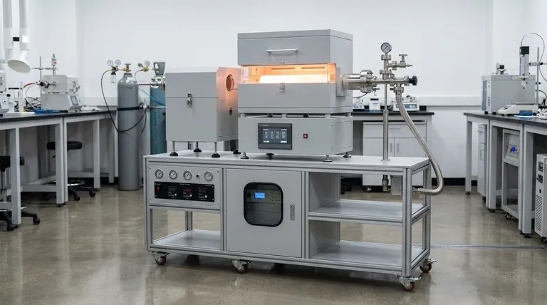
- Slide PECVD Tube Furnace with Liquid Gasifier PECVD Machine
- RF PECVD System Radio Frequency Plasma Enhanced Chemical Vapor Deposition
- Inclined Rotary Plasma Enhanced Chemical Deposition PECVD Tube Furnace Machine
- Inclined Rotary Plasma Enhanced Chemical Deposition PECVD Tube Furnace Machine
- Multi Heating Zones CVD Tube Furnace Machine for Chemical Vapor Deposition Equipment
People Also Ask
- How does PECVD equipment contribute to TOPCon bottom cells? Mastering Hydrogenation for Maximum Solar Efficiency
- What are the advantages of using a tube furnace CVD system for Cu(111)/graphene? Superior Scalability and Quality
- What is plasma in the context of PECVD? Unlock Low-Temperature Thin Film Deposition
- How does a hydrogen reduction environment in an industrial tube furnace facilitate gold-copper alloy microspheres?
- What are the disadvantages of tube furnace cracking when processing heavy raw materials? Avoid Costly Downtime and Inefficiency


