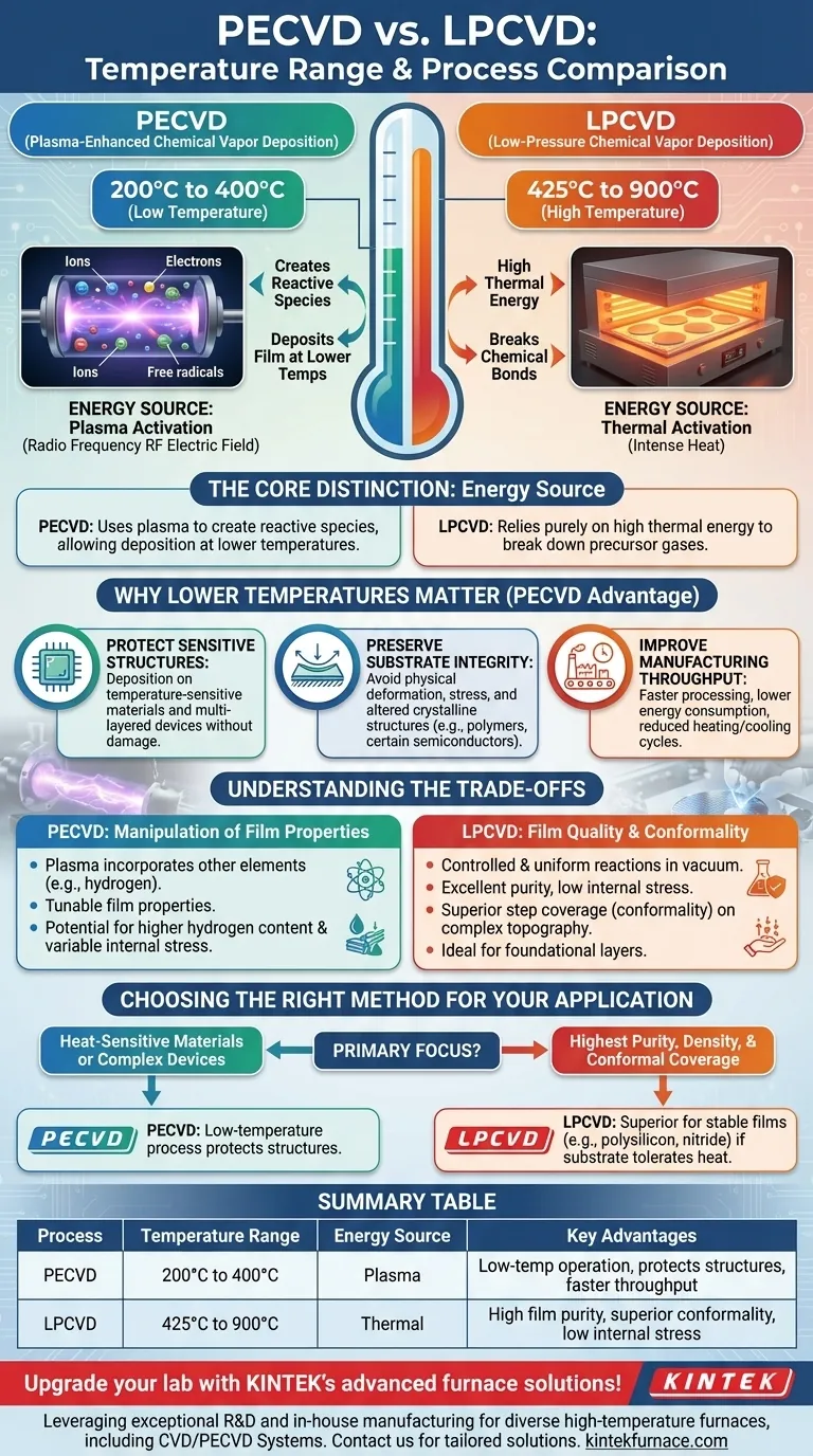
In short, Plasma-Enhanced Chemical Vapor Deposition (PECVD) operates at a significantly lower temperature range of 200°C to 400°C. In contrast, Low-Pressure Chemical Vapor Deposition (LPCVD) requires much higher temperatures, typically between 425°C and 900°C. This fundamental difference stems from how each process supplies the energy needed for the chemical reaction.
The core distinction is not just the temperature, but the energy source. LPCVD relies purely on high thermal energy to break down precursor gases, whereas PECVD uses plasma to create reactive species, allowing deposition to occur at much lower temperatures.
The Fundamental Difference: Thermal vs. Plasma Energy
To understand the temperature gap, you must first understand how each process activates the chemical reactions needed to deposit a thin film.
How LPCVD Works: Thermal Activation
LPCVD is a thermally-driven process. It operates in a vacuum furnace where wafers are heated to very high temperatures.
This intense heat provides the activation energy required to break the chemical bonds of the precursor gases, allowing them to react and deposit a solid film on the substrate surface.
How PECVD Works: Plasma Activation
PECVD replaces मौसम thermal energy with plasma energy. Inside the reaction chamber, an electric field (typically radio frequency or RF) is used to ionize the precursor gases, creating plasma.
This plasma is a highly energetic soup of ions, electrons, and free radicals. These reactive species can initiate the deposition reaction without needing the high temperatures characteristic of LPCVD.
Why Lower Temperatures Matter
The ability of PECVD to operate at lower temperatures is not just a minor detail; it is a critical advantage that enables bottlenecke fabrication of modern electronic devices.
Protecting Temperature-Sensitive Structures
Many advanced devices are built layer by layer. The components polisi already on a wafer, such as transistors or low-k dielectrics, can be damaged or degraded by the high temperatures of LPCVD.
PECVD's low-temperature window (200-400°C) allows for deposition on these partially fabricated devices without compromising njihove electrical characteristics.
Preserving Substrate Integrity
High temperatures (above 400°C) can cause physical deformation, introduce stress, or alter the crystalline structure of the underlying substrate.
This is especially critical for materials like polymers or certain compound semiconductors that simply cannot withstand the 900°C temperatures used in some LPCVD processes.
Improving Manufacturing Throughput
Lowering the process temperature reduces the time required for heating and cooling cycles within the manufacturing flow.
This reduction in "time-at-temperature" directly translates to faster processing, lower energy consumption, and higher overall factory throughput.
Understanding the Trade-offs
While low temperature is a significant advantage, the choice between PECVD and LPCVD involves balancing competing factors. Each method excels in different areas.
The LPCVD Advantage: Film Quality and Conformality
Because LPCVD relies on heat in a vacuum, the reactions are often more controlled and uniform. This typically results in films with excellent purity, low internal stress, and superior step coverage (conformality) over complex surface topography.
For foundational layers like high-quality silicon nitride or polysilicon, the high thermal budget of LPCVD is often necessary to achieve the desired material properties.
The PECVD Consideration: Film Composition and Stress
The use of plasma in PECVD can incorporate other elements, like hydrogen, from the precursor gases into the deposited film. This can be used avantageously to "passivate" surfaces or tune film properties.
However, it also means PECVD films can have higher hydrogen content and more variable internal stress, which must be carefully managed depending on the application. The process allows for more manipulation of film properties, but this requires tighter control.
Choosing the Right Method for Your Application
Your choice ultimately depends on the specific requirements of the film and the constraints of your substrate.
- If your primary focus is depositing on heat-sensitive materials or complex, multi-layered devices: PECVD is the clear choice due to its low-temperature process that protects underlying structures.
- If your primary focus is achieving the highest purity, density, and conformal coverage for stable films like polysilicon or stoichiometric nitride: LPCVD is often the superior or even necessary method, provided your substrate can tolerate the heat.
By understanding that the temperature difference is a direct result of the energy source, you can make a more informed decision based on your specific engineering goals.
Summary Table:
| Process | Temperature Range | Energy Source | Key Advantages |
|---|---|---|---|
| PECVD | 200°C to 400°C | Plasma | Low-temperature operation, protects heat-sensitive structures, faster throughput |
| LPCVD | 425°C to 900°C | Thermal | High film purity, superior conformality, low internal stress |
Upgrade your lab with KINTEK's advanced furnace solutions! Leveraging exceptional R&D and in-house manufacturing, we provide diverse laboratories with high-temperature furnaces like Muffle, Tube, Rotary, Vacuum & Atmosphere, and CVD/PECVD Systems. Our strong deep customization capability ensures we precisely meet your unique experimental needs, whether you require low-temperature PECVD for sensitive devices or high-quality LPCVD films. Contact us today to discuss how our tailored solutions can enhance your research and production efficiency!
Visual Guide
Related Products
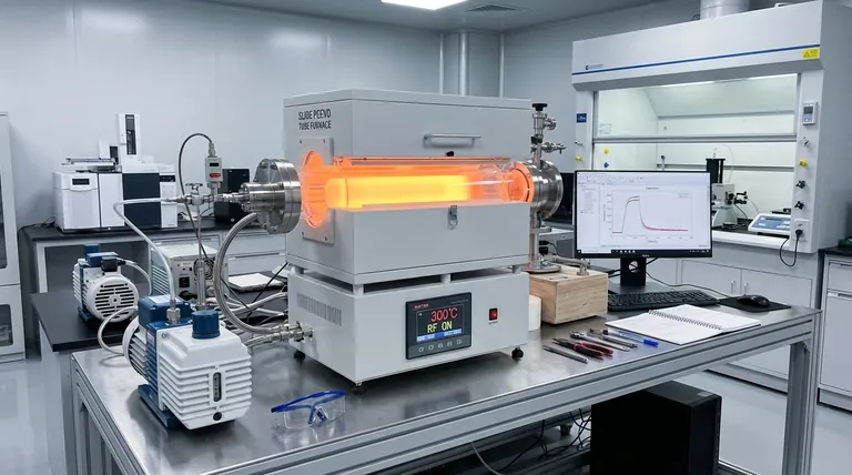
- Slide PECVD Tube Furnace with Liquid Gasifier PECVD Machine
- RF PECVD System Radio Frequency Plasma Enhanced Chemical Vapor Deposition
- Inclined Rotary Plasma Enhanced Chemical Deposition PECVD Tube Furnace Machine
- Inclined Rotary Plasma Enhanced Chemical Deposition PECVD Tube Furnace Machine
- Multi Heating Zones CVD Tube Furnace Machine for Chemical Vapor Deposition Equipment
People Also Ask
- How does a hydrogen reduction environment in an industrial tube furnace facilitate gold-copper alloy microspheres?
- What is plasma in the context of PECVD? Unlock Low-Temperature Thin Film Deposition
- What are the typical conditions for plasma-enhanced CVD processes? Achieve Low-Temperature Thin Film Deposition
- What role does a Tube Furnace play in the CVD growth of carbon nanotubes? Achieve High-Purity CNT Synthesis
- What plasma source is used in PE-CVD tube furnaces? Unlock Low-Temperature, High-Quality Deposition


