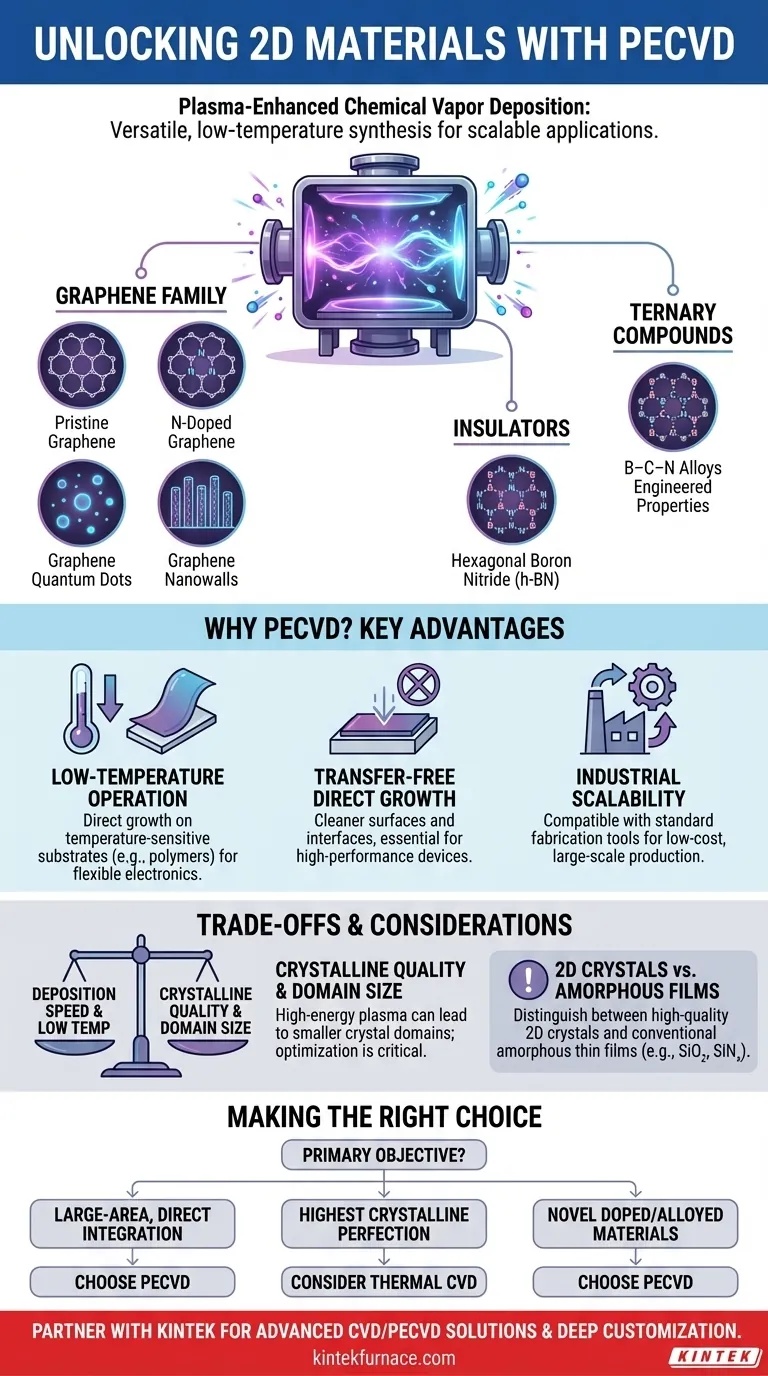
Plasma-enhanced chemical vapor deposition (PECVD) is a highly versatile technique capable of preparing several key two-dimensional (2D) materials. The process is used to synthesize pristine or nitrogen-doped graphene, graphene quantum dots, and graphene nanowalls. Beyond the graphene family, PECVD is also effective for creating hexagonal boron nitride (h-BN) and complex ternary compounds like B–C–N.
While traditional methods for synthesizing 2D materials often require high temperatures and problematic transfer steps, PECVD offers a transformative alternative. Its primary advantage is enabling low-temperature, direct growth of 2D materials on a variety of substrates, paving the way for scalable and industrially compatible manufacturing.
The Scope of PECVD for 2D Material Synthesis
PECVD uses an electric field to generate a plasma, which decomposes precursor gases at much lower temperatures than conventional thermal CVD. This energy-assisted process unlocks unique capabilities for 2D material growth and modification.
Graphene and its Derivatives
PECVD provides a high degree of control for creating various forms of graphene. It can be used to grow pristine graphene crystals or intentionally introduce other elements, such as in nitrogen-doped graphene, to tune its electronic properties.
The technique is also used to synthesize specific graphene nanostructures, such as graphene quantum dots and vertically-aligned graphene nanowalls.
Insulators and Ternary Compounds
Beyond conductors like graphene, PECVD is a proven method for synthesizing the 2D insulator hexagonal boron nitride (h-BN).
Its ability to precisely mix different precursor gases also allows for the creation of B–C–N ternary materials, which are 2D alloys with properties that can be engineered between those of graphene and h-BN.
Post-Synthesis Material Modification
PECVD is not limited to initial synthesis. A mild plasma can be used to treat or modify existing 2D materials, such as **tungsten diselenide (WSe₂) **, to functionalize their surface or repair defects without high-temperature annealing.
Why PECVD is a Compelling Choice for 2D Materials
The advantages of PECVD directly address some of the most significant challenges in making 2D materials practical for real-world applications.
Low-Temperature Operation
The use of plasma allows for material deposition at significantly lower temperatures than thermal CVD. This is critical for growing 2D materials directly on temperature-sensitive substrates like polymers, enabling flexible electronics.
Transfer-Free Direct Growth
Many high-quality 2D material synthesis methods require a separate, often damaging, step to transfer the material from a growth substrate to a target substrate. PECVD allows for transfer-free deposition, growing the material directly where it will be used.
This process results in cleaner surfaces and interfaces, which is essential for high-performance electronic and optoelectronic devices.
Industrial Scalability and Compatibility
The combination of lower temperatures, direct growth, and compatibility with standard semiconductor fabrication tools makes PECVD an attractive method for scalable and low-cost production of 2D materials.
Understanding the Trade-offs and Distinctions
While powerful, PECVD is not a universal solution. Understanding its limitations is key to making an informed decision.
Crystalline Quality vs. Deposition Speed
The high-energy plasma environment that enables low-temperature growth can sometimes lead to smaller crystal domain sizes or a higher density of defects compared to the slow, high-temperature growth of thermal CVD. Optimizing plasma conditions is critical to balance deposition speed with crystalline quality.
2D Crystals vs. Amorphous Thin Films
PECVD is widely used in industry to deposit non-crystalline (amorphous) or polycrystalline thin films like silicon dioxide (SiO₂), silicon nitride (SiNₓ), and diamond-like carbon (DLC).
It is important to distinguish this conventional use from the more advanced application of growing high-quality, single- or few-layer 2D crystals like graphene. The latter requires much more precise process control.
The Complexity of Plasma Chemistry
The plasma state is chemically complex and highly sensitive to process parameters like pressure, power, and gas flow rates. Achieving a specific, high-quality 2D material requires significant expertise and careful process optimization.
Making the Right Choice for Your Project
To determine if PECVD is the right approach, consider your primary objective.
- If your primary focus is large-area, direct device integration: PECVD's transfer-free, low-temperature process makes it an ideal candidate, especially for flexible or temperature-sensitive substrates.
- If your primary focus is achieving the highest possible crystalline perfection: You may need to compare PECVD with high-temperature thermal CVD, as the plasma environment can introduce defects if not perfectly controlled.
- If your primary focus is creating novel doped or alloyed 2D materials: PECVD offers excellent control over precursor gases, making it a powerful tool for synthesizing materials like N-doped graphene or B-C-N compounds.
By understanding these capabilities and trade-offs, you can effectively determine if PECVD is the optimal path for your specific 2D material goals.
Summary Table:
| Material Type | Examples | Key Features |
|---|---|---|
| Graphene Family | Pristine graphene, Nitrogen-doped graphene, Graphene quantum dots, Graphene nanowalls | Tunable electronic properties, nanostructure control |
| Insulators | Hexagonal boron nitride (h-BN) | High thermal stability, insulating properties |
| Ternary Compounds | B–C–N alloys | Engineered properties between graphene and h-BN |
| Post-Synthesis Modifications | Tungsten diselenide (WSe₂) | Surface functionalization, defect repair |
Unlock the potential of PECVD for your 2D material projects with KINTEK! Leveraging exceptional R&D and in-house manufacturing, we provide advanced high-temperature furnace solutions tailored for diverse laboratories. Our product line includes Muffle, Tube, Rotary Furnaces, Vacuum & Atmosphere Furnaces, and CVD/PECVD Systems, enhanced by strong deep customization capabilities to precisely meet your unique experimental requirements. Whether you're developing flexible electronics or novel materials, our expertise ensures scalable, efficient synthesis. Contact us today to discuss how we can support your innovation and drive success!
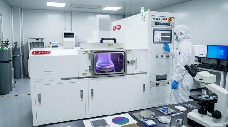
Visual Guide
Related Products
- RF PECVD System Radio Frequency Plasma Enhanced Chemical Vapor Deposition
- Inclined Rotary Plasma Enhanced Chemical Deposition PECVD Tube Furnace Machine
- Slide PECVD Tube Furnace with Liquid Gasifier PECVD Machine
- Inclined Rotary Plasma Enhanced Chemical Deposition PECVD Tube Furnace Machine
- Cylindrical Resonator MPCVD Machine System for Lab Diamond Growth
People Also Ask
- How is silicon dioxide deposited from tetraethylorthosilicate (TEOS) in PECVD? Achieve Low-Temperature, High-Quality SiO2 Films
- What are the applications of plasma enhanced chemical vapor deposition? Key Uses in Electronics, Optics & Materials
- What are some promising applications of PECVD-prepared 2D materials? Unlock Advanced Sensing and Optoelectronics
- What are the key advantages of PECVD technology? Achieve Low-Temperature, High-Quality Thin Film Deposition
- What is RF in PECVD? A Critical Control for Plasma Deposition


