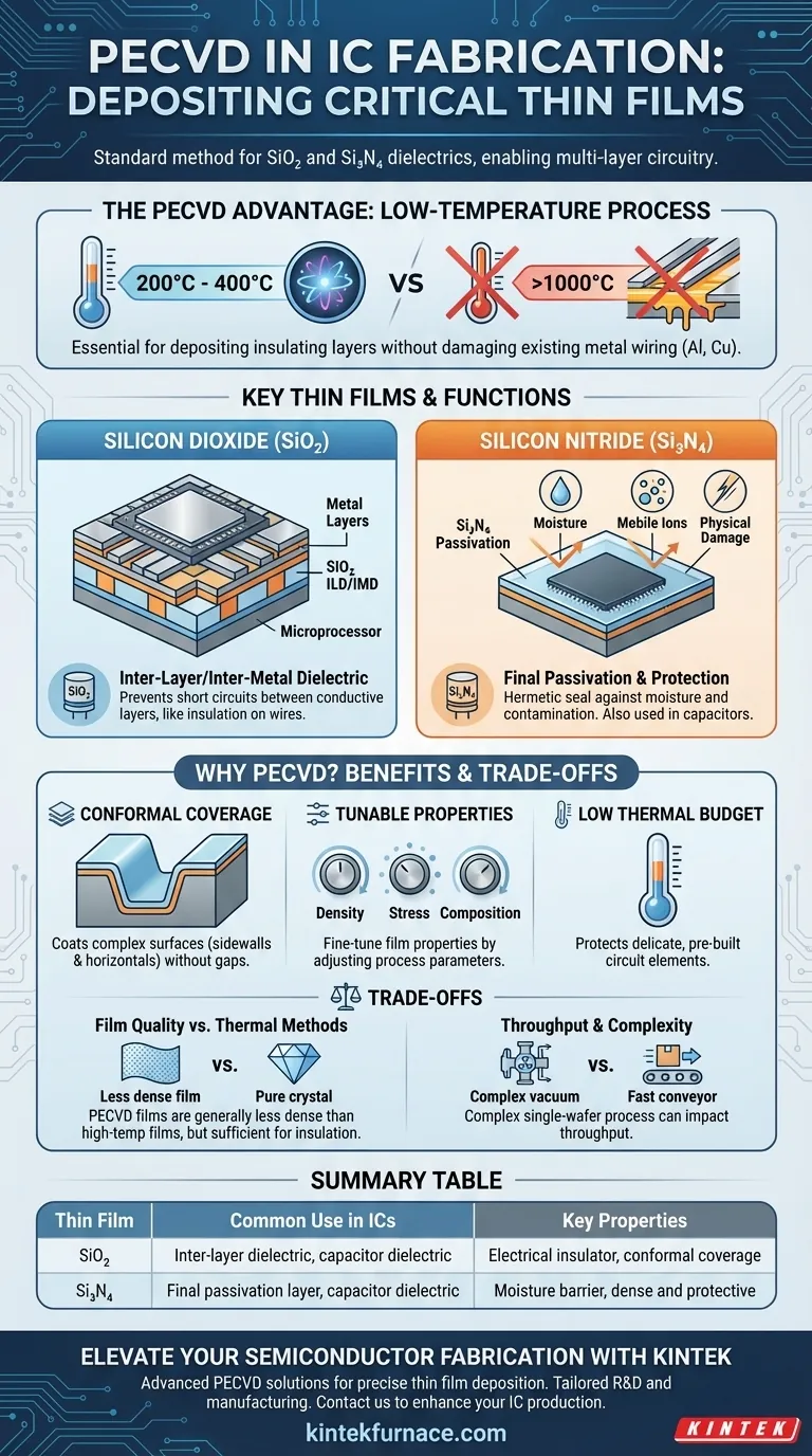
In integrated circuit (IC) fabrication, Plasma-Enhanced Chemical Vapor Deposition (PECVD) is the standard method for depositing two critical thin films: silicon dioxide (SiO₂) and silicon nitride (Si₃N₄). These materials function as essential insulators (dielectrics) that prevent short circuits between conductive layers and are used to build fundamental components like capacitors.
The crucial insight is not just what films are deposited, but why PECVD is the chosen method. Its low-temperature process is essential for depositing these insulating layers without damaging the delicate, multi-layered circuitry already built on the silicon wafer.
The Role of Dielectric Films in an IC
To understand the importance of PECVD, we must first understand the function of the films it creates. Both SiO₂ and Si₃N₄ are dielectrics, meaning they do not conduct electricity well.
Inter-Layer and Inter-Metal Dielectrics (ILD/IMD)
In a modern microprocessor, millions of transistors are wired together using a complex roadmap of up to a dozen or more metal layers.
Silicon dioxide (SiO₂) is the primary material used to fill the gaps between these metal lines, preventing them from touching and causing a catastrophic short circuit. It acts like the plastic insulation on a bundle of wires.
Final Passivation and Protection
An integrated circuit is incredibly sensitive to the outside world. Moisture, mobile ions (like sodium), and physical scratches can instantly destroy it.
Silicon nitride (Si₃N₄) serves as the chip's final protective armor. It is deposited as a tough, dense top layer that hermetically seals the device, providing excellent resistance to moisture and chemical contamination.
Capacitor Formation
Capacitors are fundamental components used for storing charge, filtering signals, and in memory cells.
A capacitor can be formed by sandwiching a dielectric film (like SiO₂ or Si₃N₄) between two conductive layers. PECVD allows for precise control over the thickness of this dielectric, which directly determines the capacitor's performance.
Why PECVD is the Preferred Method
Other deposition methods exist, but PECVD has a unique advantage that makes it indispensable in the later stages of chip manufacturing.
The Low-Temperature Advantage
The most critical benefit of PECVD is its low operating temperature, typically between 200°C and 400°C.
Earlier fabrication steps, like growing the initial gate oxide, can use high-temperature methods (over 1000°C). However, once the metal wiring layers (typically aluminum or copper) are in place, high temperatures would melt them or cause them to migrate, destroying the circuit.
PECVD bypasses this thermal budget limit by using energy from a plasma to drive the chemical reactions, rather than high heat.
Conformal Coverage
The surface of an IC is not flat; it has a complex topography of trenches and mesas. PECVD provides good conformal coverage, meaning the deposited film coats the vertical sidewalls as well as the horizontal surfaces, ensuring complete insulation without gaps.
Tunable Film Properties
By adjusting the precursor gases, RF power, and pressure within the PECVD chamber, engineers can fine-tune the properties of the film. They can control its density, internal stress, and chemical composition to meet the specific requirements of a given layer.
Understanding the Trade-offs
PECVD is a solution born of necessity, and it involves compromises. Understanding these trade-offs is key to appreciating its role.
Film Quality vs. Thermal Methods
The price for low-temperature deposition is film quality. PECVD films are generally less dense and contain more impurities (like hydrogen from precursor gases) than films grown at high temperatures. While this quality is sufficient for inter-layer insulation, it is not pure enough for the most critical transistor gate dielectric.
Throughput and Complexity
PECVD is a single-wafer, vacuum-based process. The systems are complex and expensive, and the deposition rates are slower than some alternative methods, which can impact overall manufacturing throughput.
Making the Right Choice for Your Goal
The selection between PECVD silicon dioxide and silicon nitride is entirely dependent on the film's intended function within the IC's structure.
- If your primary focus is electrical isolation between metal layers: PECVD silicon dioxide is the standard choice due to its excellent dielectric properties and ability to fill gaps effectively.
- If your primary focus is final device protection (passivation): PECVD silicon nitride is used for its superior density and exceptional barrier performance against moisture and contaminants.
Choosing the correct deposition technique for a specific material and application is a cornerstone of successful semiconductor engineering.
Summary Table:
| Thin Film | Common Use in ICs | Key Properties |
|---|---|---|
| Silicon Dioxide (SiO₂) | Inter-layer dielectric, capacitor dielectric | Electrical insulator, conformal coverage |
| Silicon Nitride (Si₃N₄) | Final passivation layer, capacitor dielectric | Moisture barrier, dense and protective |
Elevate your semiconductor fabrication with KINTEK's advanced PECVD solutions! We specialize in high-temperature furnace systems, including PECVD, designed for precise thin film deposition. Our expertise in R&D and in-house manufacturing ensures tailored solutions for your lab's unique needs, offering products like CVD/PECVD Systems with deep customization capabilities. Contact us today to discuss how we can enhance your IC production efficiency and quality!
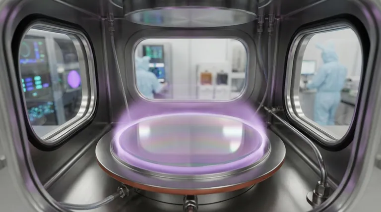
Visual Guide
Related Products
- RF PECVD System Radio Frequency Plasma Enhanced Chemical Vapor Deposition
- Slide PECVD Tube Furnace with Liquid Gasifier PECVD Machine
- Inclined Rotary Plasma Enhanced Chemical Deposition PECVD Tube Furnace Machine
- Inclined Rotary Plasma Enhanced Chemical Deposition PECVD Tube Furnace Machine
People Also Ask
- How are deposition rates and film properties controlled in PECVD? Master Key Parameters for Optimal Thin Films
- What is RF in PECVD? A Critical Control for Plasma Deposition
- What are the advantages of PECVD in film deposition? Achieve Low-Temp, High-Quality Coatings
- How does film quality compare between PECVD and CVD? Choose the Best Method for Your Substrate
- How is silicon dioxide deposited from tetraethylorthosilicate (TEOS) in PECVD? Achieve Low-Temperature, High-Quality SiO2 Films


