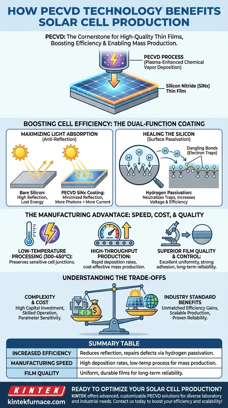
In short, Plasma-Enhanced Chemical Vapor Deposition (PECVD) is a cornerstone technology in solar cell manufacturing because it deposits high-quality thin films that serve a dual purpose. These films simultaneously boost the cell's efficiency by reducing light reflection and repairing electronic defects in the silicon, all while enabling the high-speed, low-temperature process required for cost-effective mass production.
PECVD's critical contribution is not merely the deposition of a layer, but its ability to create a multi-functional film that improves both optical and electrical properties of the solar cell in a single, industrially scalable step.
Boosting Cell Efficiency: The Dual-Function Coating
The primary role of PECVD in crystalline silicon solar cell production is to deposit a thin, precisely engineered film of silicon nitride (SiNx). This single layer dramatically improves performance in two distinct ways.
Maximizing Light Absorption (Anti-Reflection)
A bare silicon wafer is shiny and reflects a significant portion of incoming sunlight. This reflected light is lost energy that cannot be converted into electricity.
The PECVD-deposited SiNx film acts as an anti-reflection coating. By precisely controlling the film's thickness and refractive index, manufacturers can minimize reflection across the solar spectrum, ensuring more photons enter the silicon and generate current.
Healing the Silicon (Surface Passivation)
During manufacturing, the surface of a silicon wafer is left with microscopic imperfections, including "dangling bonds." These are unterminated chemical bonds that act as traps for charge carriers (electrons).
When charge carriers get trapped, they cannot contribute to the electrical current, which reduces the cell's voltage and overall efficiency.
The PECVD process for SiNx uses precursor gases rich in hydrogen. This hydrogen is incorporated into the film and diffuses a short distance into the silicon surface, where it "passivates" or neutralizes these dangling bonds. This repair of the silicon surface is a critical mechanism for achieving high-efficiency cells.
The Manufacturing Advantage: Speed, Cost, and Quality
Beyond improving the cell itself, PECVD is dominant because its process characteristics are perfectly aligned with the demands of high-volume industrial production.
Low-Temperature Processing
Traditional Chemical Vapor Deposition (CVD) requires very high temperatures, which can damage the sensitive, shallow electronic junctions of a modern solar cell.
PECVD uses an energy-rich plasma to drive the chemical reactions, allowing for film deposition at much lower temperatures (typically 300-450°C). This low-temperature processing preserves the integrity of the underlying solar cell structure.
High-Throughput Production
For solar energy to be cost-competitive, cells must be manufactured at extremely high speeds. PECVD offers a very rapid deposition rate—in some cases over 100 times faster than conventional CVD for the same material.
This high throughput, combined with modern modular systems that allow for high uptime and efficient material use, directly reduces the cost per watt of the final solar panel.
Superior Film Quality and Control
The plasma environment gives operators exceptional control over the final film's properties, including its density, stress, and chemical composition.
This results in films with excellent uniformity across the entire wafer, strong adhesion, and fewer pinholes or cracks. This reliability is essential for ensuring the 25+ year operational lifetime expected of a solar panel.
Understanding the Trade-offs
While PECVD is the industry standard, it is not without its complexities. Acknowledging these is key to understanding its place in the manufacturing line.
System Complexity and Cost
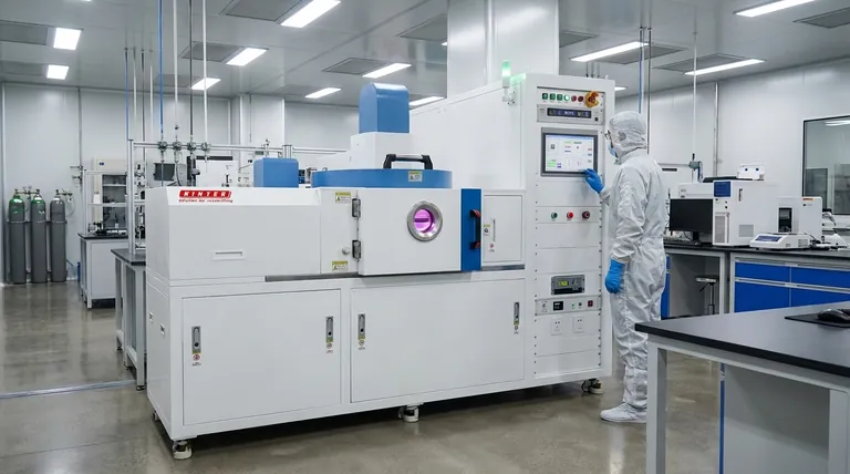
PECVD systems are sophisticated pieces of equipment involving high-vacuum chambers, precise gas flow controllers, and radio-frequency (RF) power generators. This represents a significant capital investment and requires skilled technicians to operate and maintain.
Parameter Sensitivity
The final quality of the anti-reflection and passivation layer is highly sensitive to process parameters like gas mixture, pressure, temperature, and plasma power. Any deviation can lead to suboptimal films, impacting the efficiency and yield of the entire production line. This necessitates robust process control and monitoring.
How to Apply This to Your Goal
Your focus determines which aspect of PECVD is most relevant to you.
- If your primary focus is R&D or cell efficiency: The key is PECVD's ability to control film properties and deliver hydrogen for excellent surface passivation, which are critical levers for pushing cell voltage and efficiency higher.
- If your primary focus is manufacturing and scale-up: The crucial benefits are the high deposition rate, low-temperature compatibility, and high system uptime, which enable cost-effective, high-volume production.
- If your primary focus is long-term reliability: The value lies in PECVD's ability to produce dense, stable, and uniform films that protect the cell and perform consistently for decades in the field.
Ultimately, PECVD has become indispensable because it elegantly solves both scientific and economic challenges in solar cell manufacturing.
Summary Table:
| Benefit | Description |
|---|---|
| Increased Efficiency | Reduces light reflection and repairs silicon defects via hydrogen passivation. |
| Manufacturing Speed | High deposition rates and low-temperature processing for cost-effective mass production. |
| Film Quality | Produces uniform, durable films with precise control for long-term reliability. |
Ready to optimize your solar cell production with advanced PECVD solutions? KINTEK leverages exceptional R&D and in-house manufacturing to provide diverse laboratories with high-temperature furnace solutions, including CVD/PECVD Systems. Our strong deep customization capability ensures we precisely meet your unique experimental requirements. Contact us today to discuss how our tailored PECVD technologies can boost your efficiency and scalability!
Visual Guide
Related Products
- Slide PECVD Tube Furnace with Liquid Gasifier PECVD Machine
- RF PECVD System Radio Frequency Plasma Enhanced Chemical Vapor Deposition
- Inclined Rotary Plasma Enhanced Chemical Deposition PECVD Tube Furnace Machine
- Inclined Rotary Plasma Enhanced Chemical Deposition PECVD Tube Furnace Machine
- Multi Heating Zones CVD Tube Furnace Machine for Chemical Vapor Deposition Equipment
People Also Ask
- What are the main advantages of PECVD tube furnaces compared to CVD tube furnaces? Lower Temp, Faster Deposition, and More
- What are the advantages of using a tube furnace CVD system for Cu(111)/graphene? Superior Scalability and Quality
- What plasma source is used in PE-CVD tube furnaces? Unlock Low-Temperature, High-Quality Deposition
- What are the typical conditions for plasma-enhanced CVD processes? Achieve Low-Temperature Thin Film Deposition
- What is plasma in the context of PECVD? Unlock Low-Temperature Thin Film Deposition


