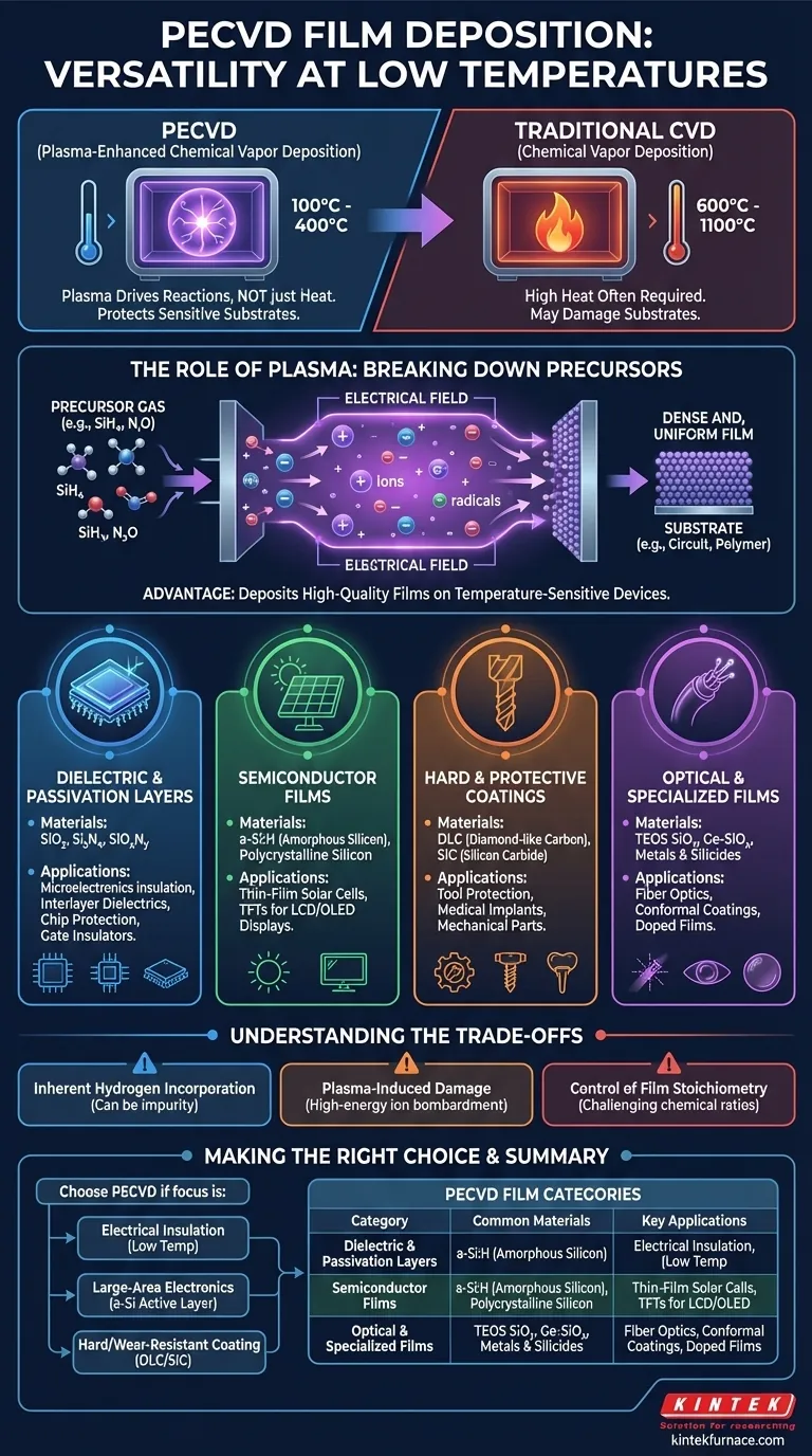
In short, Plasma-Enhanced Chemical Vapor Deposition (PECVD) is a highly versatile technique capable of depositing a wide range of thin films. The most common materials include dielectrics like silicon dioxide (SiO₂) and silicon nitride (Si₃N₄), semiconductor films such as amorphous silicon (a-Si:H), and hard protective coatings like diamond-like carbon (DLC) and silicon carbide (SiC).
The fundamental advantage of PECVD is its ability to deposit high-quality, dense, and uniform films at significantly lower temperatures than traditional Chemical Vapor Deposition (CVD). This makes it the go-to method for coating temperature-sensitive substrates or devices with existing structures.
Why PECVD Excels: The Role of Plasma
The key to PECVD's capabilities lies in its use of plasma to drive chemical reactions, rather than relying solely on high thermal energy. This distinction is the source of its primary benefits.
Breaking Down Precursors at Low Temperatures
In a PECVD system, an electrical field is used to ionize precursor gases, creating a reactive plasma. This plasma contains a mix of ions, electrons, and highly reactive free radicals.
These energized species can react and form a solid film on a substrate at temperatures typically between 100°C and 400°C. This is a dramatic reduction from the 600°C to 1100°C often required for thermal CVD processes.
Protecting Temperature-Sensitive Substrates
The low-temperature nature of PECVD is its most critical feature. It allows for the deposition of films on substrates that would be damaged or destroyed by high heat.
This includes completed integrated circuits with aluminum or copper metallization, polymer-based flexible electronics, and various optical components.
A Breakdown of Common PECVD Films
The versatility of PECVD is best understood by categorizing the types of films it can produce. Each category serves a distinct set of industrial and research applications.
Dielectric and Passivation Layers
This is the most common application for PECVD. These insulating films are crucial for manufacturing microelectronics.
Materials include silicon dioxide (SiO₂), silicon nitride (Si₃N₄), and silicon oxynitride (SiOxNy). They are used as interlayer dielectrics, final passivation layers to protect chips from moisture and contamination, and as gate insulators in transistors.
Semiconductor Films
PECVD is a dominant technology for depositing active semiconductor layers, particularly for large-area electronics.
The most notable material is hydrogenated amorphous silicon (a-Si:H), which forms the active layer in many thin-film solar cells and thin-film transistors (TFTs) used in LCD displays. The process also allows for the deposition of polycrystalline silicon.
Hard and Protective Coatings
The high ion energy in the plasma can be leveraged to create exceptionally hard and durable films.
Diamond-like carbon (DLC) films are prized for their extreme hardness, low friction coefficient, and chemical inertness, making them ideal for protecting tools, medical implants, and mechanical components. Silicon carbide (SiC) offers similar benefits with high thermal stability.
Optical and Specialized Films
The precise control over film properties allows for specialized applications. PECVD can produce TEOS SiO₂ (from a tetraethyl orthosilicate precursor), known for its excellent ability to conformally coat and fill gaps in complex topographies.
It can also be used to create doped films, such as germanium-doped silicon oxide (Ge-SiOx) for fiber optics, or even deposit certain metals and their silicides.
Understanding the Trade-offs
While powerful, PECVD is not without its complexities. An expert must understand its limitations to deploy it effectively.
Inherent Hydrogen Incorporation
Because many precursor gases are hydrogen-based (e.g., silane, SiH₄), hydrogen atoms are often incorporated into the deposited film. While this is essential for passivating defects in amorphous silicon (a-Si:H), it can be an unwanted impurity in other films, potentially affecting their electrical or optical properties.
Potential for Plasma-Induced Damage
The high-energy ions that drive the deposition reaction can also bombard the substrate surface. This can induce stress, create defects in the underlying material, or damage sensitive electronic device structures. Careful process tuning is required to balance deposition rate with minimizing damage.
Control of Film Stoichiometry
Achieving a precise chemical ratio (stoichiometry) in complex films like silicon oxynitride (SiOxNy) can be challenging. The final composition depends on a complex interplay of gas flows, pressure, plasma power, and temperature, requiring careful process development and characterization.
Making the Right Choice for Your Goal
Selecting a deposition method depends entirely on the film's purpose and the substrate's limitations. PECVD should be your primary consideration under these circumstances.
- If your primary focus is electrical insulation on a completed device: PECVD is the industry standard for depositing SiO₂ and Si₃N₄ passivation layers due to its low process temperature.
- If your primary focus is manufacturing large-area electronics like displays or solar cells: PECVD is the essential technology for creating high-quality amorphous silicon active layers.
- If your primary focus is a hard, wear-resistant coating on a mechanical part: PECVD is a superior choice for depositing DLC or SiC films with excellent adhesion and durability.
- If your primary focus is achieving the highest possible crystal quality or film purity: You may need to consider higher-temperature methods like thermal CVD or molecular-beam epitaxy (MBE), provided your substrate can withstand the heat.
Ultimately, PECVD is a cornerstone of modern materials engineering, empowering the creation of advanced films on virtually any substrate.
Summary Table:
| Film Category | Common Materials | Key Applications |
|---|---|---|
| Dielectric Layers | SiO₂, Si₃N₄, SiOxNy | Microelectronics insulation, passivation |
| Semiconductor Films | a-Si:H, polycrystalline silicon | Solar cells, TFTs in displays |
| Protective Coatings | DLC, SiC | Hard coatings for tools, medical implants |
| Optical Films | TEOS SiO₂, Ge-SiOx | Fiber optics, conformal coatings |
Unlock the potential of PECVD for your laboratory with KINTEK's advanced solutions! Leveraging exceptional R&D and in-house manufacturing, we provide high-temperature furnaces like CVD/PECVD Systems tailored for diverse labs. Our deep customization capability ensures precise fit for unique experimental needs, helping you deposit superior thin films efficiently. Contact us today to discuss how we can enhance your research and production processes!
Visual Guide
Related Products
- RF PECVD System Radio Frequency Plasma Enhanced Chemical Vapor Deposition
- Slide PECVD Tube Furnace with Liquid Gasifier PECVD Machine
- Inclined Rotary Plasma Enhanced Chemical Deposition PECVD Tube Furnace Machine
- Inclined Rotary Plasma Enhanced Chemical Deposition PECVD Tube Furnace Machine
People Also Ask
- How does film quality compare between PECVD and CVD? Choose the Best Method for Your Substrate
- What are the applications of plasma enhanced chemical vapor deposition? Key Uses in Electronics, Optics & Materials
- What is PECVD specification? A Guide to Choosing the Right System for Your Lab
- What is RF in PECVD? A Critical Control for Plasma Deposition
- What are some promising applications of PECVD-prepared 2D materials? Unlock Advanced Sensing and Optoelectronics


