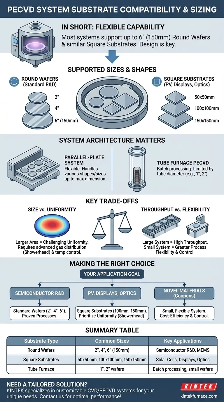
In short, most research and development PECVD systems accommodate a range of substrate sizes, typically supporting standard circular wafers up to 6 inches (150 mm) in diameter as well as square substrates of similar dimensions. However, the exact size is not a universal standard and is fundamentally determined by the specific system's chamber design and hardware configuration.
The critical takeaway is that "wafer size" is often shorthand for a system's maximum substrate area. You must look beyond a single diameter measurement and consider the system's compatibility with both round wafers and square substrates to ensure it aligns with your specific fabrication requirements.
Unpacking PECVD Substrate Compatibility
When evaluating a Plasma-Enhanced Chemical Vapor Deposition (PECVD) system, understanding its substrate capacity is about more than just a single number. It involves the shape, the range of sizes, and the underlying architecture of the tool itself.
Standard Round Wafer Sizes
Most PECVD systems used in semiconductor and MEMS research are built around standard silicon wafer sizes. The most common maximum size for these platforms is 6 inches (or 150 mm) in diameter.
These systems are typically designed to handle smaller wafers as well, often accommodating 2-inch and 4-inch wafers with simple carrier platens or tooling adjustments.
Support for Square Substrates
Many applications, particularly in fields like solar cells, displays, or specialized optics, use square or rectangular substrates.
PECVD platforms are frequently designed to support these form factors. Common supported sizes include 50 mm x 50 mm, 100 mm x 100 mm, and 150 mm x 150 mm, which correspond roughly to the 2, 4, and 6-inch wafer diameters.
The Role of System Architecture
The physical design of the PECVD system is the ultimate constraint. A parallel-plate system with a large, flat lower electrode (platen) can often handle various shapes up to its maximum dimension.
In contrast, a tube furnace PECVD is designed for batches of wafers arranged vertically in a quartz tube. These are inherently limited to the tube's diameter, with common sizes being designed for 1-inch and 2-inch wafers.
Understanding the Trade-offs: Size vs. Uniformity
Selecting a system based on size involves critical performance trade-offs. A larger chamber does not automatically mean better results, especially for smaller samples.
The Challenge of Uniformity
As the substrate size increases, maintaining uniform deposition becomes significantly more difficult. Achieving consistent film thickness, refractive index, and stress across a 6-inch area requires sophisticated process control.
This includes precise temperature management across the platen and advanced gas distribution, often using a "showerhead" design to ensure the precursor gases are delivered evenly.
Throughput vs. Flexibility
Larger systems offer higher throughput, allowing you to coat a larger area or more wafers at once.
However, smaller, dedicated systems can offer greater flexibility for process development and may provide tighter control for novel materials research on smaller, coupon-sized samples. Running a small sample in a large chamber can be inefficient and may compromise process results if not properly configured.
Making the Right Choice for Your Application
To ensure you select a compatible and effective system, you must align the machine's capabilities with your primary research or production goal.
- If your primary focus is standard semiconductor R&D: Look for systems explicitly supporting common wafer sizes like 2-inch, 4-inch, and 6-inch, as these will have proven processes and tooling.
- If your primary focus is photovoltaics, displays, or optics: Prioritize systems that specify compatibility with square substrates (e.g., 100 mm x 100 mm or 150 mm x 150 mm) and have showerhead gas injection for uniformity.
- If your primary focus is novel materials on small coupons: A smaller, more flexible system may offer better cost-efficiency and process control than a large-area platform.
Ultimately, you must verify the system's chamber and platen specifications against your exact substrate dimensions to guarantee compatibility.
Summary Table:
| Substrate Type | Common Sizes Supported | Key Applications |
|---|---|---|
| Round Wafers | 2", 4", 6" (150 mm) | Semiconductor R&D, MEMS |
| Square Substrates | 50x50 mm, 100x100 mm, 150x150 mm | Solar Cells, Displays, Optics |
| Tube Furnace PECVD | 1", 2" wafers | Batch processing for small wafers |
Need a PECVD system tailored to your unique substrate requirements? KINTEK specializes in advanced high-temperature furnace solutions, including CVD/PECVD systems, with strong deep customization capabilities to precisely match your experimental needs. Whether you're in semiconductor R&D, photovoltaics, or optics, our expertise in R&D and in-house manufacturing ensures optimal performance and flexibility. Contact us today to discuss how we can enhance your lab's efficiency and results!
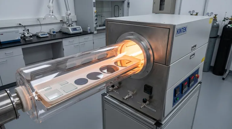
Visual Guide
Related Products
- RF PECVD System Radio Frequency Plasma Enhanced Chemical Vapor Deposition
- Slide PECVD Tube Furnace with Liquid Gasifier PECVD Machine
- Inclined Rotary Plasma Enhanced Chemical Deposition PECVD Tube Furnace Machine
- Inclined Rotary Plasma Enhanced Chemical Deposition PECVD Tube Furnace Machine
- Cylindrical Resonator MPCVD Machine System for Lab Diamond Growth
People Also Ask
- How does film quality compare between PECVD and CVD? Choose the Best Method for Your Substrate
- What is PECVD specification? A Guide to Choosing the Right System for Your Lab
- What are the key advantages of PECVD technology? Achieve Low-Temperature, High-Quality Thin Film Deposition
- What is the role of RF power in PECVD and how does the RF-PECVD process work? Master Thin Film Deposition Control
- What are some promising applications of PECVD-prepared 2D materials? Unlock Advanced Sensing and Optoelectronics


