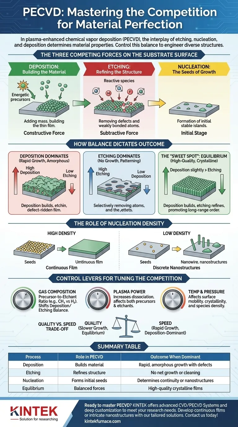
In plasma-enhanced chemical vapor deposition (PECVD), the simultaneous competition between etching, nucleation, and deposition is the fundamental mechanism that enables precise control over material preparation. This dynamic balance is not a flaw in the process; it is the very feature that allows for the creation of materials with diverse, tailored morphologies and properties, from continuous films to intricate nanostructures.
The final outcome of a PECVD process is determined by the delicate balance between adding material (deposition), removing it (etching), and initiating its growth (nucleation). Mastering PECVD means learning how to intentionally shift this balance to achieve a specific material structure.
The Three Competing Forces in PECVD
To control the outcome of a PECVD process, you must first understand the three core actions that are constantly at war with each other on the substrate surface.
### Deposition: Building the Material
Deposition is the primary growth mechanism. Energetic and reactive chemical precursors from the plasma land on the substrate and bond to it, adding mass and building the thin film layer by layer. This is the constructive force in the system.
### Etching: Refining the Structure
Simultaneously, other reactive species in the plasma—often atomic hydrogen or fluorine—act as etchants. They bombard the growing film and selectively remove weakly bonded atoms, amorphous phases, or misaligned crystals. This subtractive force purifies the material and helps define its structure.
### Nucleation: The Seeds of Growth
Before significant deposition can occur, the process must begin with nucleation. This is the formation of the first stable, tiny islands of material on the substrate. The density and distribution of these initial nuclei are critical; they dictate whether the film will grow as a continuous sheet or as a collection of separate structures.
How the Balance Dictates the Outcome
The final morphology of the material is a direct result of which of these three processes is dominant at any given moment.
### When Deposition Dominates
If the deposition rate far outpaces the etching rate, growth is rapid. This can be useful for creating thick, amorphous films quickly. However, without the refining action of etching, the resulting material often has more defects and a less-ordered crystalline structure.
### When Etching Dominates
If the etching rate is greater than the deposition rate, no net film growth will occur. In extreme cases, the plasma will begin to etch the substrate itself. This regime is only desirable when the goal is to pattern or clean a surface, not to grow a film.
### The "Sweet Spot": Deposition-Etching Equilibrium
The key to growing high-quality crystalline films lies in finding a state of near-equilibrium. Here, the deposition rate is only slightly higher than the etching rate. Deposition builds the crystal lattice, while the constant etching "cleans up" any atoms that don't land in the correct spot, removing defects and promoting long-range order.
### The Role of Nucleation Density
The initial nucleation phase sets the stage for the final morphology.
- High Nucleation Density: Many seeds form close together, leading them to quickly merge (coalesce) into a uniform, continuous film.
- Low Nucleation Density: Fewer, widely-spaced seeds form, allowing each one to grow into a distinct, isolated structure like a nanowire, nanodisk, or vertical graphene sheet before it touches its neighbor.
Understanding the Trade-offs and Control Parameters
Your ability to control the PECVD process hinges on your ability to manipulate the parameters that shift the balance between these competing forces.
### Control Lever: Gas Composition
This is the most direct lever. The ratio of precursor gas (e.g., methane for carbon growth) to etchant gas (e.g., hydrogen) directly controls the deposition-vs-etching balance. More precursor favors deposition; more etchant favors etching.
### Control Lever: Plasma Power
Increasing plasma power generally increases the dissociation of all gases, creating more precursors and more etchants. This can accelerate both deposition and etching, and its net effect is highly dependent on the specific gas chemistry and pressure.
### Control Lever: Temperature and Pressure
Higher substrate temperatures provide atoms with more surface mobility, helping them find their ideal lattice sites and promoting crystallinity. System pressure affects the density and energy of the plasma species, altering the dominant reactions in the chamber.
### The Quality vs. Speed Trade-off
There is an inherent trade-off. Conditions that favor extremely high-quality crystalline materials (a finely-tuned deposition-etching balance) often require slower growth rates. Conversely, achieving rapid growth usually requires a deposition-dominant regime, which can sacrifice crystalline quality.
Tuning the Competition for Your Goal
Use your understanding of this dynamic competition to achieve your specific material synthesis objective.
- If your primary focus is high-quality, continuous crystalline films: Your goal is a delicate equilibrium where the deposition rate is just slightly higher than the etching rate to allow for defect removal.
- If your primary focus is rapid, amorphous film growth: You should operate in a deposition-dominant regime by increasing the precursor-to-etchant gas ratio.
- If your primary focus is creating discrete nanostructures (e.g., nanowires, islands): You must control the initial nucleation phase to achieve a low density of nucleation sites, allowing structures to grow separately.
- If your primary focus is material patterning or surface cleaning: You must intentionally create an etching-dominant regime by using a high concentration of etchant gas and minimal or no precursor gas.
By viewing these competing forces as controllable levers, you can transform the PECVD process from a complex challenge into a precise tool for materials engineering.
Summary Table:
| Process | Role in PECVD | Outcome When Dominant |
|---|---|---|
| Deposition | Builds material by adding atoms | Rapid growth, often amorphous with defects |
| Etching | Refines structure by removing atoms | No net growth or surface cleaning |
| Nucleation | Forms initial growth seeds | Determines film continuity or nanostructure formation |
| Equilibrium | Balanced deposition and etching | High-quality crystalline films with defect removal |
Ready to master PECVD for your material synthesis? KINTEK leverages exceptional R&D and in-house manufacturing to provide advanced high-temperature furnace solutions, including CVD/PECVD Systems. Our strong deep customization capability ensures we precisely meet your unique experimental requirements, whether you're developing continuous films or intricate nanostructures. Contact us today to discuss how our tailored solutions can enhance your lab's efficiency and achieve superior material outcomes!
Visual Guide
Related Products
- Slide PECVD Tube Furnace with Liquid Gasifier PECVD Machine
- RF PECVD System Radio Frequency Plasma Enhanced Chemical Vapor Deposition
- Inclined Rotary Plasma Enhanced Chemical Deposition PECVD Tube Furnace Machine
- Inclined Rotary Plasma Enhanced Chemical Deposition PECVD Tube Furnace Machine
- Multi Heating Zones CVD Tube Furnace Machine for Chemical Vapor Deposition Equipment
People Also Ask
- In which industries is the tube furnace commonly used? Essential for Materials Science, Energy, and More
- What are the advantages of using a tube furnace CVD system for Cu(111)/graphene? Superior Scalability and Quality
- What is plasma in the context of PECVD? Unlock Low-Temperature Thin Film Deposition
- How does a hydrogen reduction environment in an industrial tube furnace facilitate gold-copper alloy microspheres?
- What plasma source is used in PE-CVD tube furnaces? Unlock Low-Temperature, High-Quality Deposition


