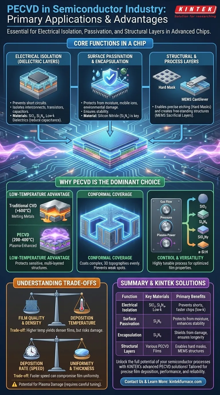
In the semiconductor industry, Plasma-Enhanced Chemical Vapor Deposition (PECVD) is primarily used to deposit thin films that serve three critical functions: electrical isolation between conductive layers, passivation to protect device surfaces, and encapsulation to shield the final chip from environmental damage. These films, such as silicon dioxide and silicon nitride, are fundamental building blocks in virtually all modern microelectronic devices.
The essential value of PECVD is its ability to deposit high-quality, functional films at low temperatures. This single advantage allows complex, multi-layered chips to be built without damaging sensitive, previously fabricated structures, a limitation that would otherwise halt modern semiconductor manufacturing.
The Core Functions of PECVD Films in a Chip
PECVD films are not just ancillary components; they are integral to a device's structure, performance, and long-term reliability. Their applications can be categorized by their primary function within the integrated circuit.
Electrical Isolation (Dielectric Layers)
The most common application is creating insulating layers that prevent electrical "short circuits." As transistors and wires are packed closer together, these dielectric films are crucial.
PECVD-deposited silicon dioxide (SiO₂) and silicon nitride (Si₃N₄) are used to isolate metal interconnects, transistors, and capacitors from one another.
This technique is also used for depositing low-k dielectric materials, which are specialized insulators that reduce parasitic capacitance between wires, enabling faster chip speeds and lower power consumption.
Surface Passivation and Encapsulation
Semiconductor materials, especially silicon, are highly sensitive to contamination. PECVD films act as a protective barrier.
Passivation layers are deposited early in the process to protect the active silicon surface from moisture and mobile ions that could alter the device's electrical characteristics. Silicon nitride is a common choice due to its excellent barrier properties.
Later in the manufacturing flow, encapsulation films are deposited to protect the entire finished device from physical damage, corrosion, and moisture ingress, ensuring its stability and longevity.
Structural and Process-Enabling Layers
Beyond their electrical and protective roles, PECVD films are also used as temporary or permanent structural elements during fabrication.
They can be used as hard masks, which are durable stencils that define the patterns to be etched into underlying layers with high precision.
In Micro-Electro-Mechanical Systems (MEMS), PECVD films can be deposited as sacrificial layers that are later removed to create free-standing mechanical structures like cantilevers or membranes.
Why PECVD is the Dominant Choice
Other deposition methods exist, but PECVD's unique process characteristics make it indispensable for modern, high-density chip manufacturing. The "plasma-enhanced" aspect is the key differentiator.
The Low-Temperature Advantage
This is the most critical benefit of PECVD. Traditional Chemical Vapor Deposition (CVD) often requires temperatures above 600°C, which would melt or damage the delicate aluminum or copper interconnects already built on the chip.
PECVD uses an energy-rich plasma to break down precursor gases, allowing the chemical reactions needed for film deposition to occur at much lower temperatures, typically 200-400°C.
This low-temperature budget is what makes it possible to build devices with many layers of complex, temperature-sensitive circuitry.
Conformal Coverage for Complex Geometries
Modern chips are not flat. They feature deep trenches and towering vertical structures. A deposited film must be able to coat these complex topographies evenly.
PECVD provides excellent conformal coverage, meaning the film maintains a uniform thickness over the tops, bottoms, and sidewalls of these features. This prevents weak spots or gaps in insulation.
Control and Versatility
The PECVD process is highly tunable. By adjusting parameters like gas flow, pressure, and plasma power, engineers can precisely control the properties of the deposited film.
This allows for the creation of a wide variety of materials, including silicon dioxide (SiO₂), silicon nitride (Si₃N₄), silicon oxynitride (SiOxNy), and amorphous silicon (a-Si:H), each optimized for a specific application.
Understanding the Trade-offs
While powerful, PECVD is not without its compromises. Engineers must balance competing factors to achieve their desired outcome.
Film Quality vs. Temperature
While the low-temperature process is a key advantage, PECVD films can sometimes contain higher concentrations of hydrogen compared to films grown at higher temperatures. This can affect the film's density and electrical properties.
Generally, there is a trade-off between the deposition temperature and the "purity" or density of the film.
Deposition Rate vs. Uniformity
PECVD is known for its relatively fast deposition rates, which is good for manufacturing throughput. However, pushing for the highest possible speed can sometimes compromise the film's thickness uniformity across the entire wafer.
This requires careful process tuning to find the optimal balance between manufacturing speed and consistent device performance.
Potential for Plasma Damage
The energetic plasma that enables low-temperature deposition can also, in some cases, induce damage to the sensitive transistor gates or other delicate structures on the wafer's surface.
Process engineers work to mitigate this by carefully designing the reactor and tuning the plasma conditions to minimize this effect.
Making the Right Choice for Your Goal
The specific PECVD film and process are chosen based on the primary objective for that particular layer in the chip design.
- If your primary focus is performance and speed: Your best choice is a low-k dielectric film deposited by PECVD between metal interconnects to minimize signal delay.
- If your primary focus is device reliability: You will rely on dense silicon nitride films deposited by PECVD for passivation and encapsulation to protect against moisture and contaminants.
- If your primary focus is fabricating 3D structures: The conformal deposition capabilities of PECVD are essential for uniformly coating complex topographies in advanced logic, memory, or MEMS devices.
Ultimately, PECVD's ability to deposit essential films at manageable temperatures makes it an indispensable tool that enables the relentless miniaturization and increasing complexity of all modern electronics.
Summary Table:
| Function | Key Materials | Primary Benefits |
|---|---|---|
| Electrical Isolation | Silicon Dioxide (SiO₂), Silicon Nitride (Si₃N₄), Low-k Dielectrics | Prevents short circuits, reduces capacitance for faster chips |
| Surface Passivation | Silicon Nitride (Si₃N₄) | Protects from moisture and ions, enhances device stability |
| Encapsulation | Silicon Nitride (Si₃N₄) | Shields chips from environmental damage, ensures longevity |
| Structural Layers | Various PECVD Films | Enables hard masks and sacrificial layers in MEMS fabrication |
Unlock the full potential of your semiconductor processes with KINTEK's advanced PECVD solutions! Leveraging exceptional R&D and in-house manufacturing, we provide diverse laboratories with high-temperature furnace systems, including CVD/PECVD Systems, tailored to your unique needs. Our deep customization capabilities ensure precise film deposition for enhanced device performance and reliability. Contact us today to discuss how our expertise can elevate your research and production!
Visual Guide
Related Products
- RF PECVD System Radio Frequency Plasma Enhanced Chemical Vapor Deposition
- Inclined Rotary Plasma Enhanced Chemical Deposition PECVD Tube Furnace Machine
- Slide PECVD Tube Furnace with Liquid Gasifier PECVD Machine
- Inclined Rotary Plasma Enhanced Chemical Deposition PECVD Tube Furnace Machine
- 915MHz MPCVD Diamond Machine Microwave Plasma Chemical Vapor Deposition System Reactor
People Also Ask
- What are the advantages of PECVD in film deposition? Achieve Low-Temp, High-Quality Coatings
- What is PECVD specification? A Guide to Choosing the Right System for Your Lab
- How is silicon dioxide deposited from tetraethylorthosilicate (TEOS) in PECVD? Achieve Low-Temperature, High-Quality SiO2 Films
- What is the role of RF power in PECVD and how does the RF-PECVD process work? Master Thin Film Deposition Control
- What are some promising applications of PECVD-prepared 2D materials? Unlock Advanced Sensing and Optoelectronics


