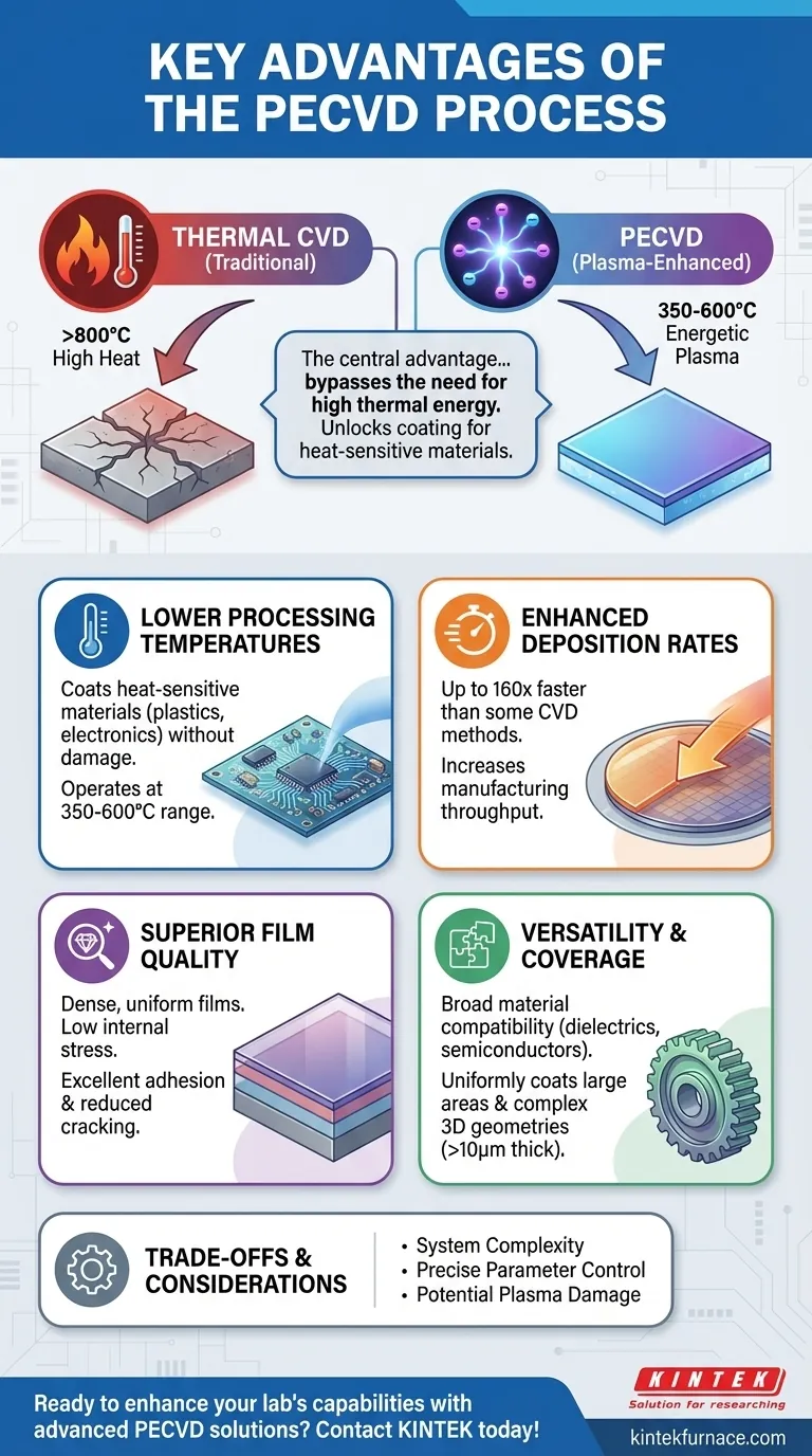
At its core, Plasma-Enhanced Chemical Vapor Deposition (PECVD) is a process that fundamentally changes the energy requirements for film deposition. Its key advantages are the ability to operate at significantly lower temperatures than conventional CVD, deposit a wide variety of high-quality films with low internal stress, and achieve much faster deposition rates, making it a highly versatile and efficient manufacturing tool.
The central advantage of PECVD is its use of plasma to energize precursor gases, which bypasses the need for high thermal energy. This single principle unlocks the ability to coat heat-sensitive materials and dramatically improves the efficiency and quality of the deposition process.
The Fundamental Advantage: Bypassing Thermal Energy with Plasma
Traditional Chemical Vapor Deposition (CVD) relies on high temperatures (often >800°C) to provide the energy needed for chemical reactions to occur on a substrate's surface. PECVD offers a more elegant solution by using an electric field to create plasma, an ionized gas containing energetic electrons.
Lower Processing Temperatures
These highly energetic electrons—not high heat—transfer energy to the precursor gas molecules. This allows for film deposition at much lower substrate temperatures, typically in the 350-600°C range.
This capability is critical for depositing films on temperature-sensitive substrates, such as plastics, polymers, or complex electronic devices that would be damaged or destroyed by conventional CVD temperatures.
Enhanced Deposition Rates
The plasma environment dramatically accelerates chemical reactions. This allows for significantly higher deposition rates compared to thermal processes.
For some materials, like silicon nitride, PECVD can be up to 160 times faster than low-pressure CVD. This translates directly to increased manufacturing throughput.
Superior Film Quality and Versatility
The unique, energy-rich environment of PECVD allows for the creation of films with desirable properties that are often difficult to achieve with other methods.
High-Quality and Uniform Films
PECVD produces films that are dense and uniform, with fewer pinholes and a reduced tendency to crack. The process provides excellent adhesion of the film to the substrate.
Low Internal Stress
Films grown via PECVD generally exhibit low internal stress. This is crucial for performance and reliability, as high stress can cause films to delaminate, crack, or warp the underlying substrate.
Broad Material Compatibility
PECVD is an exceptionally versatile technique. It can be used to deposit a wide range of materials, including dielectrics (like silicon dioxide and silicon nitride), semiconductors (like amorphous silicon), and even some metals and polymer-like coatings.
Excellent Substrate Coverage
The process is well-suited for coating large-area substrates uniformly. It can also effectively coat parts with complex 3D geometries, providing better three-dimensional coverage than line-of-sight methods like Physical Vapor Deposition (PVD). Furthermore, PECVD can create very thick coatings (greater than 10 μm), a capability often limited in other deposition techniques.
Understanding the Trade-offs
While powerful, PECVD is not without its complexities. Acknowledging these trade-offs is key to making an informed decision.
System Complexity
PECVD systems are inherently more complex than thermal CVD reactors. They require RF or microwave power sources, impedance matching networks, and more sophisticated process control, which can increase initial equipment cost and maintenance.
Process Parameter Control
The quality of a PECVD film is highly dependent on a wide array of parameters, including gas composition, flow rate, pressure, RF power, and frequency. Optimizing a process requires careful tuning of these interconnected variables.
Potential for Plasma Damage
The same energetic ions that enable low-temperature deposition can, if not properly controlled, cause damage to the surface of a sensitive substrate or the growing film itself. This requires careful process design to balance reaction enhancement with damage mitigation.
Making the Right Choice for Your Goal
The decision to use PECVD should be driven by the specific requirements of your substrate and desired film properties.
- If your primary focus is coating heat-sensitive materials: PECVD is the definitive choice, as its low-temperature operation protects substrates that traditional CVD would destroy.
- If your primary focus is high throughput and efficiency: PECVD's rapid deposition rates offer a clear advantage for mass production over slower thermal methods.
- If your primary focus is film integrity and performance: The ability to produce low-stress, well-adhered, and crack-resistant films makes PECVD ideal for demanding applications.
- If your primary focus is material versatility: PECVD provides a single platform capable of depositing a vast range of dielectric, semiconducting, and protective coatings.
By leveraging plasma instead of brute-force heat, PECVD provides a level of control and capability that opens new possibilities in materials engineering.
Summary Table:
| Advantage | Key Benefit |
|---|---|
| Lower Processing Temperatures | Enables coating of heat-sensitive substrates (e.g., plastics, electronics) without damage |
| Enhanced Deposition Rates | Up to 160x faster than some CVD methods, boosting manufacturing throughput |
| Superior Film Quality | Produces dense, uniform films with low internal stress and excellent adhesion |
| Broad Material Compatibility | Deposits dielectrics, semiconductors, and more on various substrates |
| Excellent Substrate Coverage | Uniformly coats large areas and complex 3D geometries with thick layers (>10 μm) |
Ready to enhance your lab's capabilities with advanced PECVD solutions? At KINTEK, we leverage exceptional R&D and in-house manufacturing to provide diverse laboratories with cutting-edge high-temperature furnace systems, including our specialized CVD/PECVD Systems. Our strong deep customization capability ensures we precisely meet your unique experimental needs, whether you're working with heat-sensitive materials or aiming for higher throughput. Contact us today to discuss how our tailored PECVD solutions can drive your research and production forward!
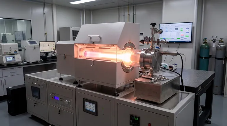
Visual Guide
Related Products
- RF PECVD System Radio Frequency Plasma Enhanced Chemical Vapor Deposition
- Slide PECVD Tube Furnace with Liquid Gasifier PECVD Machine
- Inclined Rotary Plasma Enhanced Chemical Deposition PECVD Tube Furnace Machine
- Inclined Rotary Plasma Enhanced Chemical Deposition PECVD Tube Furnace Machine
- Multi Heating Zones CVD Tube Furnace Machine for Chemical Vapor Deposition Equipment
People Also Ask
- What is RF in PECVD? A Critical Control for Plasma Deposition
- What are the key advantages of PECVD technology? Achieve Low-Temperature, High-Quality Thin Film Deposition
- What are the advantages of PECVD in film deposition? Achieve Low-Temp, High-Quality Coatings
- What are the applications of plasma enhanced chemical vapor deposition? Key Uses in Electronics, Optics & Materials
- What is the role of RF power in PECVD and how does the RF-PECVD process work? Master Thin Film Deposition Control


