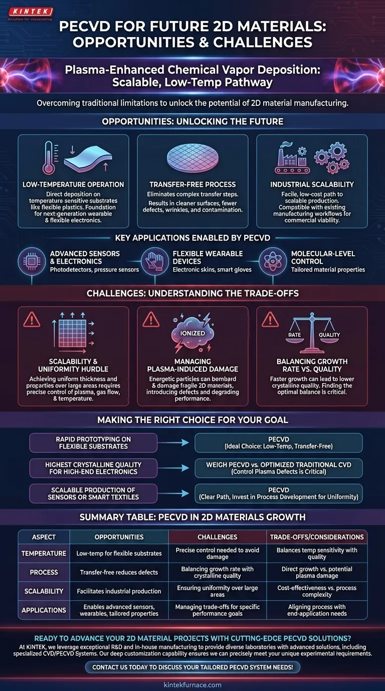
For the future of 2D materials, Plasma-Enhanced Chemical Vapor Deposition (PECVD) represents a pivotal opportunity for scalable, low-temperature manufacturing. This method allows for the direct growth of materials on a wide variety of substrates, offering clear advantages over traditional Chemical Vapor Deposition (CVD). However, realizing its full potential requires overcoming key challenges in process control and material quality.
While traditional methods are hampered by high temperatures and damaging transfer steps, PECVD offers a direct, low-temperature pathway to manufacturing 2D materials. The central challenge lies in refining the plasma process to achieve large-scale uniformity and high crystalline quality without sacrificing these core benefits.
The Core Advantage: Overcoming Traditional CVD Limitations
PECVD's primary value is that it directly solves the most significant bottlenecks associated with conventional growth methods for 2D materials.
Low-Temperature Operation
Traditional CVD often requires extremely high temperatures, limiting its use to robust, temperature-insensitive substrates.
PECVD operates at much lower temperatures. This crucial difference unlocks the ability to deposit 2D materials directly onto temperature-sensitive substrates like flexible plastics, making it foundational for next-generation wearable and flexible electronics.
A Transfer-Free Process
With many traditional methods, the 2D material must be grown on a catalytic metal foil and then painstakingly transferred to the final device substrate.
This transfer step is a major source of defects, wrinkles, and contamination. PECVD eliminates this step by growing the material directly on the target substrate, resulting in cleaner surfaces and interfaces.
Industrial Compatibility and Scalability
The combination of lower temperatures and a simpler, transfer-free process makes PECVD inherently more compatible with existing industrial manufacturing workflows.
This provides a direct, facile, and low-cost path to scalable production, which is essential for commercial viability.
Key Opportunities and Applications
The advantages of PECVD enable a new class of devices and applications that were previously difficult or impossible to manufacture at scale.
Advanced Sensors and Electronics
The ability to produce high-quality 2D material films allows for the creation of highly sensitive devices.
Promising applications already demonstrated in prototypes include photodetectors, pressure sensors, and biochemical sensors.
The Foundation for Flexible and Wearable Devices
PECVD is the key enabling technology for functional, large-area flexible electronics.
Real-world examples include distributed pressure sensor arrays for electronic skins, touch modules on robotic hands capable of recognizing braille, and smart gloves that can record and translate sign language.
Molecular-Level Control for Tailored Properties
PECVD is a mature technology in other fields, such as the production of high-quality diamond films, because it offers precise control.
This molecular-level control over film properties is indispensable for developing cutting-edge technologies, allowing engineers to fine-tune material characteristics for specific applications.
Understanding the Challenges and Trade-offs
Despite its immense potential, PECVD is not a simple drop-in solution. Adopting it requires a clear understanding of its inherent technical challenges.
The Challenge of Scalability and Uniformity
While PECVD is described as scalable, achieving this in practice is a significant engineering hurdle.
Ensuring the uniformity of the material's thickness and properties over a large area (e.g., an entire wafer) requires extremely precise control over the plasma, gas flow, and temperature.
Managing Plasma-Induced Damage
The "plasma" in PECVD is an ionized gas containing high-energy particles. This is what allows for low-temperature deposition.
However, if not perfectly managed, these energetic particles can bombard and damage the fragile 2D material as it grows, introducing defects that can degrade its electronic or optical performance.
Balancing Growth Rate vs. Crystalline Quality
There is often a trade-off between the speed of deposition and the quality of the resulting material.
Pushing for faster growth to improve manufacturing throughput can lead to a less-ordered, lower-quality crystalline structure. Finding the optimal balance for a given application is a critical part of process development.
Making the Right Choice for Your Goal
To leverage PECVD effectively, you must align the process with your primary objective.
- If your primary focus is rapid prototyping on flexible substrates: PECVD is an ideal choice due to its low-temperature and transfer-free capabilities.
- If your primary focus is achieving the highest possible crystalline quality for high-end electronics: You must carefully weigh PECVD against optimized traditional CVD, as controlling plasma-induced defects is critical to performance.
- If your primary focus is scalable production of sensors or smart textiles: PECVD offers a clear path forward, but expect to invest significant effort in process development to ensure uniformity and yield.
Ultimately, mastering PECVD is about controlling a complex interplay of forces to unlock the next generation of 2D material devices.
Summary Table:
| Aspect | Opportunities | Challenges |
|---|---|---|
| Temperature | Low-temperature operation enables use on flexible substrates | Requires precise control to avoid plasma-induced damage |
| Process | Transfer-free growth reduces defects and contamination | Balancing growth rate with crystalline quality |
| Scalability | Facilitates industrial-scale production for cost-effectiveness | Ensuring uniformity over large areas |
| Applications | Enables advanced sensors, wearable devices, and tailored material properties | Managing trade-offs for specific performance goals |
Ready to advance your 2D material projects with cutting-edge PECVD solutions?
At KINTEK, we leverage exceptional R&D and in-house manufacturing to provide diverse laboratories with advanced high-temperature furnace solutions, including our specialized CVD/PECVD Systems. Our strong deep customization capability ensures we can precisely meet your unique experimental requirements, whether you're developing flexible electronics, sensors, or other innovative applications.
Contact us today to discuss how our tailored PECVD systems can help you overcome challenges and seize opportunities in scalable 2D material growth!
Visual Guide
Related Products
- RF PECVD System Radio Frequency Plasma Enhanced Chemical Vapor Deposition
- Slide PECVD Tube Furnace with Liquid Gasifier PECVD Machine
- Inclined Rotary Plasma Enhanced Chemical Deposition PECVD Tube Furnace Machine
- Inclined Rotary Plasma Enhanced Chemical Deposition PECVD Tube Furnace Machine
- Cylindrical Resonator MPCVD Machine System for Lab Diamond Growth
People Also Ask
- What are the applications of plasma enhanced chemical vapor deposition? Key Uses in Electronics, Optics & Materials
- What are the key advantages of PECVD technology? Achieve Low-Temperature, High-Quality Thin Film Deposition
- What are the advantages of PECVD in film deposition? Achieve Low-Temp, High-Quality Coatings
- What are the system specifications of the PECVD system? Unlock Precision Thin-Film Deposition
- What are some promising applications of PECVD-prepared 2D materials? Unlock Advanced Sensing and Optoelectronics


