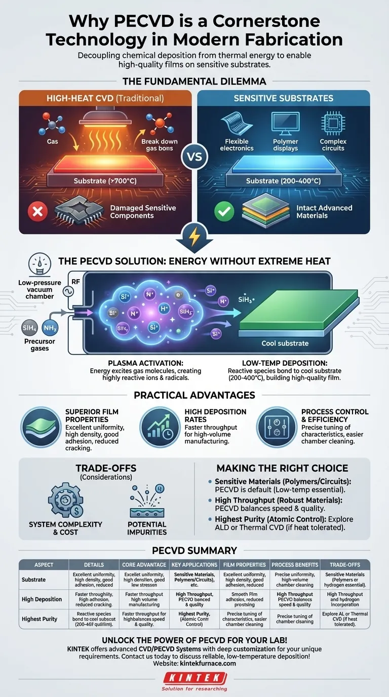
In essence, Plasma-Enhanced Chemical Vapor Deposition (PECVD) is a cornerstone technology because it solves a fundamental manufacturing dilemma: how to deposit a high-quality, durable thin film onto a surface without destroying that surface with high heat. By using an energy-rich plasma instead of extreme temperatures to drive chemical reactions, PECVD enables the creation of advanced materials on temperature-sensitive components, a capability that is indispensable for modern electronics, optics, and solar cells.
The critical advantage of PECVD is its ability to decouple the energy required for chemical deposition from thermal energy. It substitutes the brute force of high heat with the targeted energy of a plasma, enabling high-quality film growth at low temperatures.
The Fundamental Problem: Heat vs. Material Integrity
The High-Temperature Dilemma of Traditional CVD
Conventional Chemical Vapor Deposition (CVD) is a powerful technique that relies on high temperatures—often several hundred to over a thousand degrees Celsius. This thermal energy is necessary to break down precursor gases and trigger the chemical reactions that form a solid film on a substrate.
While effective, this reliance on heat creates a major limitation.
The Challenge of Sensitive Substrates
Modern fabrication, especially in semiconductors and flexible electronics, involves building complex, multi-layered structures. The underlying components, such as integrated circuits with fine metal lines or polymer-based flexible displays, cannot withstand the extreme temperatures of traditional CVD without being damaged or completely destroyed.
This creates a critical bottleneck: you cannot add a necessary functional layer if the process of adding it ruins the work you have already done.
How PECVD Solves the Heat Problem
Introducing Plasma: Energy Without Extreme Heat
PECVD circumvents the heat problem by introducing energy in a different form. Inside a low-pressure vacuum chamber, an electrical field is applied to the precursor gases.
This applied energy excites the gas molecules, stripping electrons and creating a plasma—a highly reactive state of matter consisting of ions, electrons, and neutral radicals.
The Mechanism of Plasma-Enhanced Deposition
These newly formed ions and radicals within the plasma are extremely chemically reactive. They don't need high thermal energy to react and form a film because they are already in an "activated" state.
When these activated species come into contact with the comparatively cool substrate surface, they readily bond to it, building up the desired thin film layer by layer. The process typically uses precursor gases like silane (SiH₄) for silicon films or ammonia (NH₃) for nitride films.
Key Outcome: High-Quality Films on Cool Substrates
The result is the best of both worlds. You achieve the dense, uniform, and high-quality films characteristic of a vapor deposition process, but at temperatures low enough (e.g., 200-400°C) to be compatible with sensitive, fully-fabricated devices.
The Practical Advantages of PECVD
Superior Film Properties
Because the energy is supplied by the plasma, the process allows for fine control over the film's final properties. PECVD films are known for their excellent uniformity across large substrates, high density, and good adhesion.
This process also produces films with lower internal stress, which significantly reduces the likelihood of cracking—a critical factor for device reliability.
High Deposition Rates
The highly reactive nature of the plasma species often leads to faster film growth compared to other low-temperature deposition techniques. This high throughput is a major advantage in high-volume manufacturing environments like semiconductor fabrication plants.
Process Control and Efficiency
Engineers can precisely tune film characteristics like composition, thickness, and refractive index by adjusting process parameters such as gas flow rates, pressure, and the power applied to generate the plasma. Furthermore, the process chemistry can lead to easier chamber cleaning, reducing equipment downtime.
Understanding the Trade-offs
System Complexity and Cost
PECVD systems are inherently more complex than simple thermal CVD reactors. They require sophisticated radio-frequency (RF) or microwave power supplies, vacuum technology, and precise gas handling, which can increase capital and maintenance costs.
Potential for Impurities
The energetic plasma can sometimes sputter material from the chamber walls or electrodes, which may then be incorporated into the growing film as an impurity. Additionally, precursor gases (like silane) are hydrogen-rich, and this hydrogen can be incorporated into the film, sometimes affecting its electrical or optical properties if not managed.
Making the Right Choice for Your Goal
Selecting a deposition method depends entirely on the specific requirements of your substrate and final device.
- If your primary focus is fabricating on heat-sensitive materials (like polymers, plastics, or completed circuits): PECVD is often the default choice, as its low-temperature nature is essential for preventing substrate damage.
- If your primary focus is maximizing manufacturing throughput for robust materials: PECVD provides an excellent balance of high deposition rates and high-quality film properties, making it a workhorse for mass production.
- If your primary focus is achieving the absolute highest film purity or atomic-level control: You may need to explore alternatives like Atomic Layer Deposition (ALD) or use traditional CVD if your substrate can tolerate the heat.
Ultimately, PECVD's ability to enable high-quality material deposition without destructive heat is what makes it a profoundly enabling technology for building the next generation of advanced devices.
Summary Table:
| Aspect | Details |
|---|---|
| Core Advantage | Deposits high-quality thin films at low temperatures (200-400°C) using plasma energy, avoiding substrate damage. |
| Key Applications | Semiconductors, flexible electronics, optics, solar cells. |
| Film Properties | Excellent uniformity, high density, good adhesion, low stress, reduced cracking. |
| Process Benefits | High deposition rates, precise control over film characteristics, compatibility with sensitive materials. |
| Trade-offs | Higher system complexity and cost, potential for impurities like hydrogen incorporation. |
Unlock the Power of PECVD for Your Lab!
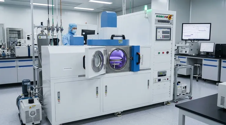
At KINTEK, we leverage exceptional R&D and in-house manufacturing to provide advanced high-temperature furnace solutions, including our specialized CVD/PECVD Systems. Our strong deep customization capability ensures we can precisely meet your unique experimental requirements, whether you're working with semiconductors, optics, or other sensitive materials.
Contact us today to discuss how our PECVD systems can enhance your fabrication processes with reliable, low-temperature deposition and boost your lab's efficiency!
Visual Guide
Related Products
- Slide PECVD Tube Furnace with Liquid Gasifier PECVD Machine
- RF PECVD System Radio Frequency Plasma Enhanced Chemical Vapor Deposition
- Inclined Rotary Plasma Enhanced Chemical Deposition PECVD Tube Furnace Machine
- Inclined Rotary Plasma Enhanced Chemical Deposition PECVD Tube Furnace Machine
- Multi Heating Zones CVD Tube Furnace Machine for Chemical Vapor Deposition Equipment
People Also Ask
- What are the advantages of using a tube furnace CVD system for Cu(111)/graphene? Superior Scalability and Quality
- What are the typical conditions for plasma-enhanced CVD processes? Achieve Low-Temperature Thin Film Deposition
- What plasma source is used in PE-CVD tube furnaces? Unlock Low-Temperature, High-Quality Deposition
- In which industries is the tube furnace commonly used? Essential for Materials Science, Energy, and More
- What are the main advantages of PECVD tube furnaces compared to CVD tube furnaces? Lower Temp, Faster Deposition, and More


