All Questions
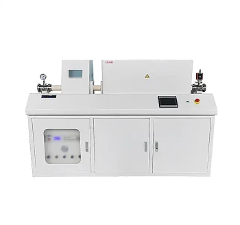
What Is The Mechanism Of The Rf Source In Pecvd? Mastering Low-Temp 2D Material Synthesis
Learn how RF sources in PECVD ionize gases into plasma to synthesize high-quality 2D materials like graphene at low temperatures (150°C–500°C).
What Is The Function Of A Pecvd System In The Passivation Of Umg Silicon Solar Cells? Enhance Efficiency With Hydrogen
Learn how PECVD systems improve UMG silicon solar cells through bulk passivation, defect repair, and advanced anti-reflective coatings.
Why Is A High-Precision Pecvd System Required In Acsm? Enable Low-Temperature Atomic-Scale Manufacturing
Learn how high-precision PECVD enables atomic-scale additive manufacturing by protecting sensitive substrates and ensuring film uniformity.
Why Is Metal Ion Pretreatment Necessary For Hipims Hlppn? Unlock Superior Nitrogen Diffusion And Surface Activation
Learn why metal ion pretreatment is vital for HIPIMS enhanced nitriding to remove oxides, implant ions, and enable deep nitrogen diffusion.
Why Is A High-Precision Pulsed Power Supply Required For Hipims Nitriding? Unlock Advanced Surface Engineering
Learn why high-precision pulsed power is critical for HIPIMS nitriding to achieve high ionization, prevent overheating, and ensure uniformity.
What Is The Function Of An Industrial-Grade Four-Cathode System In Hipims? Optimize Coatings For Complex Geometries
Learn how four-cathode systems in HIPIMS nitriding eliminate shadowing and ensure uniform, high-density coatings on complex 3D industrial parts.
Why Use Pecvd For Monolithic Integrated Chip Isolation Layers? Protect Your Thermal Budget With High-Quality Sio2
Learn how PECVD systems enable low-temperature deposition of SiO2 isolation layers to prevent leakage currents and protect sensitive chip components.
Why Is High-Purity Graphite And Acetylene Used For Dlc? Master The Sp2/Sp3 Ratio For Superior Surface Performance
Learn how the hybrid use of graphite targets and acetylene gas enables precise control over DLC coating hardness, friction, and durability.
What Is The Function Of Pulsed Dc Bias Control During Ion Etching? Master Dlc Coating Adhesion & Surface Activation
Learn how pulsed DC bias control accelerates argon ions to remove oxides and activate tool steel for superior DLC coating adhesion and durability.
How Do Multi-Channel Mass Flow Controllers (Mfc) Manage Dlc Coating Gases? Precision Flow For Superior Adhesion
Learn how multi-channel MFCs manage Argon, Nitrogen, and Acetylene to create high-performance Diamond-Like Carbon (DLC) coatings through gas gradients.
How Does A Pecvd System Contribute To (N)Poly-Si Layers? High-Throughput In-Situ Doping Explained
Learn how PECVD systems enable (n)poly-Si deposition through low-temperature plasma decomposition, uniform in-situ doping, and high-speed growth.
What Is The Role Of Lpcvd In Acm-Bn Synthesis? Master Phase Transitions With Precise Thermal Control
Learn how LPCVD systems regulate temperature profiles and precursor flow to synthesize high-quality amorphous-crystalline mixed boron nitride.
Why Is Pecvd For Silicon Nitride Deposition Essential In Gas Sensor Test Structures? Ensure Reliable Signal Isolation
Learn why PECVD Si3N4 is critical for gas sensor insulation, overcoming surface roughness challenges and ensuring electrical signal integrity.
How Does Pecvd Equipment Contribute To Topcon Bottom Cells? Mastering Hydrogenation For Maximum Solar Efficiency
Learn how PECVD equipment drives hydrogenation in TOPCon cells, neutralizing defects and extending carrier lifetime for superior solar performance.
What Are The Advantages Of Ion Bombardment Deposition For Cogeneration Impellers? Enhance Durability & Thermal Stress
Discover how ion bombardment deposition creates dense nanocrystalline coatings to prevent peeling and thermal stress on cogeneration impellers.
How Does The Microarc Produced By Ion Discharge Function? Enhance Coating Bonding Strength Via Surface Activation
Learn how microarc ion discharge improves PVD coating adhesion by removing oxide films and moisture to create atomic-level bonding.
What Is The Primary Function Of A Vacuum Pump In Pecvd Gan Synthesis? Optimize Purity And Control
Learn how high-performance vacuum pumps ensure high-purity Gallium Nitride (GaN) growth by removing contaminants and controlling plasma dynamics.
What Is The Function Of The R.f. Source In Pecvd For Gan Thin Film Synthesis? Enable Low-Temp High-Efficiency Deposition
Learn how the 13.56 MHz R.F. source in PECVD drives GaN synthesis at lower temperatures by generating reactive plasma for high-energy reactions.
How Does A Pacvd System Prepare Friction-Reducing Layers? Enhance Surface Lubricity With Plasma-Assisted Cvd
Learn how PACVD uses plasma glow discharge and precursors like Tetramethylsilane to deposit low-friction DLC:Si coatings on composite surfaces.
What Is The Purpose Of Sinx Layer Deposition Via Pecvd? Enhance Optical & Electrical Performance
Learn how PECVD-deposited SiNx layers provide anti-reflective coating and hydrogen passivation to boost device efficiency and carrier lifetime.
What Technical Advantages Does A Plasma Enhanced Chemical Vapor Deposition (Pecvd) System Offer? | Kintek
Learn how PECVD systems enable low-temperature SiNx deposition, superior hydrogen passivation, and precise refractive index control for semiconductors.
What Environments Does A Pecvd System Provide For Silicon Nanowires? Optimize Growth With Precise Thermal Control
Learn how PECVD systems provide reactive hydrogen plasma and low-energy gas-phase environments to condition catalysts for silicon nanowire growth.
What Is The Critical Application Of Pecvd Equipment In Passivated Contact Solar Cells? Boosting Efficiency With Precision
Learn how PECVD equipment deposits doped silicon into nanopinholes for passivated contact solar cells, ensuring high conductivity and efficiency.
How Does A Radio Frequency (Rf) Plasma-Enhanced Horizontal Tube Furnace Contribute To The Synthesis Of Ga2O3 Thin Films?
Learn how RF plasma-enhanced furnaces use atomic oxygen radicals to accelerate Ga2O3 thin film synthesis with superior efficiency and control.
What Are The Applications Of Inline Pecvd In Solar Cell Passivation? Maximize Efficiency With Precision Thin-Film Layers
Learn how Inline PECVD optimizes solar cells through SiNx, AlOx, and a-Si:H deposition for superior passivation and anti-reflection performance.
How Does Methane And Hydrogen Plasma Treatment Affect The Formation Of Germanium Nanocrystals (Ge Ncs)?
Learn how CH4/H2 plasma creates a carbon-rich diffusion barrier to drive Ge NC formation on a-SiC:H surfaces.
What Are The Technical Specifications For The Capacitively Coupled Dual-Electrode Pecvd Configuration? Expert Standards
Learn the essential specs for PECVD dual-electrode setups: 62x62mm geometry, 32mm gap, and 13.56 MHz RF power for uniform thin film deposition.
Why Is In-Situ Pecvd And Vacuum Evaporation Needed For Ge Ncs In A-Sic:h? Ensure Pristine Material Interfaces
Learn why integrating PECVD and vacuum evaporation in one chamber is vital to prevent oxidation and contamination in Ge NCs and a-SiC:H films.
What Is The Primary Role Of Pecvd In A-Sic:h Film Preparation? Low-Temp Precision For Advanced Thin Films
Learn how PECVD systems enable low-temperature deposition (400°C) and precise bandgap tuning for high-quality a-SiC:H thin films.
How Is A Plasma Enhanced Chemical Vapor Deposition (Pecvd) System Utilized In The Preparation Of Microcavity Sensors?
Learn how PECVD systems engineer internal stress in thin films to drive the self-rolling fabrication of high-precision 3D microcavity sensors.
Why Is The Vacuum Reaction Chamber Critical For Pecvd On Titanium Alloys? Precision Control For Superior Coatings
Learn how vacuum chambers in PECVD ensure high-purity, uniform coatings on titanium alloys by preventing atmospheric contamination and oxidation.
What Role Does A Pecvd System Play In Enhancing Nanopore Protection? Secure Nanostructures With Pecvd
Learn how PECVD uses the 'blooming effect' to create protective caps for nanopores, preventing membrane fracture during aggressive etching.
Why Is Precise Nh3/Sih4 Gas Flow Ratio Necessary For Sin Films In Single Photon Emitters? Optimize Stoichiometry Now
Learn how the R value (NH3:SiH4) controls SiN film stoichiometry, refractive index, and fluorescence for high-performance single photon emitters.
What Are The Advantages Of Pecvd Vs Traditional Cvd For Sin Films? Unlock Low-Temperature Thin Film Excellence
Learn why PECVD is superior for Silicon Nitride (SiN) growth, offering lower temperatures, CMOS compatibility, and better film control than thermal CVD.
What Is The Deposition Pressure Range For Pecvd Equipment? Optimize Film Quality And Deposition Speed
Learn the PECVD pressure range (0.133-40 Pa) and how it affects film density, deposition rate, and quality for better process control.
What Are The Specifications Of The Vacuum System In Pecvd Equipment? Optimize Your Thin-Film Deposition Process
Explore key PECVD vacuum system specs, including turbomolecular and rotary vane pumps, for high vacuum performance in semiconductor and research labs.
What Gases Are Supplied In The Pecvd Gas Supply System? Optimize Your Thin Film Deposition Process
Learn about PECVD gases like Silane, Ammonia, and CF4 for precise thin film deposition and chamber cleaning in semiconductor and optics labs.
What Are The Characteristics Of The Vacuum Chamber In Pecvd Equipment? Key Features For Superior Thin Film Deposition
Explore the essential characteristics of PECVD vacuum chambers, including stainless steel construction, electrode design, and plasma control for high-quality thin films at low temperatures.
What Are The Specifications Of The Radio Frequency Power Supply In Pecvd Equipment? Optimize Plasma Control For Superior Film Deposition
Explore key RF power supply specs for PECVD, including 13.56 MHz frequency, power output up to 500W, stability, and reflected power for precise plasma engineering.
What Are The Key Features Of Pecvd Equipment? Unlock Low-Temperature Thin Film Deposition
Explore PECVD equipment's key features like RF plasma, vacuum chambers, and precise gas control for low-temperature, high-quality thin film deposition.
How Does Pecvd Equipment Work? Unlock Low-Temperature Thin Film Deposition
Learn how PECVD equipment uses plasma for low-temperature thin film deposition, enabling precise control on heat-sensitive substrates.
What Are The Main Applications Of Pecvd Technology? Discover Versatile Thin-Film Solutions For Modern Industries
Explore PECVD technology's key uses in semiconductors, solar cells, and protective coatings, enabling low-temperature, high-quality thin-film deposition for diverse applications.
What Is Plasma Enhanced Chemical Vapor Deposition (Pecvd) Technology? Unlock Low-Temp Thin Film Deposition
Discover how PECVD enables low-temperature, high-quality thin film deposition for electronics and material science, with benefits like superior film density and versatility.
How Does Pecvd Contribute To Semiconductor Manufacturing? Enable Low-Temperature, High-Quality Film Deposition
Discover how PECVD enables low-temperature deposition of insulating films in semiconductor manufacturing, protecting sensitive layers and advancing chip fabrication.
What Role Does Plasma Play In The Pecvd Process? Enable Low-Temperature Thin-Film Deposition
Learn how plasma in PECVD replaces high heat with electrical energy for efficient thin-film growth on temperature-sensitive substrates.
Why Is Pecvd Particularly Useful For Temperature-Sensitive Substrates? Achieve Low-Temperature, High-Quality Film Deposition
Discover how PECVD enables film deposition on heat-sensitive substrates like polymers and semiconductors at 200-400°C, preventing thermal damage while maintaining coating quality.
How Is The Pecvd Process Controlled And Optimized? Master Thin Film Deposition For Your Lab
Learn how to control plasma power, gas flow, pressure, and temperature in PECVD to optimize thin film properties like thickness, density, and uniformity.
What Are The Key Steps Involved In The Pecvd Process? Master Low-Temperature Thin Film Deposition
Learn the 5 key steps of PECVD for low-temperature thin film deposition, ideal for semiconductors, solar cells, and temperature-sensitive materials.
What Factors Should Be Considered When Selecting Between Cvd And Pecvd? Choose The Right Deposition Method For Your Lab
Learn key factors like temperature, film properties, and cost to select between CVD and PECVD for optimal thin-film deposition in your applications.
What Are The Limitations Of Pecvd Compared To Cvd? Key Trade-Offs In Film Quality And Performance
Explore the drawbacks of PECVD vs. CVD, including softer films, lower density, and potential impurities, to optimize your deposition process.
What Advantages Does Pecvd Offer Over Cvd? Lower Temperatures, Broader Applications
Discover PECVD's key benefits over CVD: lower processing temperatures, broader substrate compatibility, and enhanced film control for modern applications.
What Materials Can Be Used As Coatings In Pecvd? Explore Versatile Thin-Film Solutions For Your Lab
Discover PECVD coatings like silicon dioxide, diamond-like carbon, and polymers for microelectronics, medical devices, and more with low-temperature processing.
What Are The Advantages Of Pecvd-Deposited Films? Achieve Superior Film Quality At Low Temperatures
Discover the benefits of PECVD films, including low-temperature deposition, superior uniformity, and precise control for semiconductors, optics, and MEMS applications.
What Is Plasma-Enhanced Chemical Vapor Deposition (Pecvd) And How Does It Differ From Cvd? Unlock Low-Temperature Thin Film Deposition
Explore PECVD vs. CVD: Learn how plasma enables low-temperature thin film deposition for sensitive substrates, with key differences in energy sources and applications.
What Is Plasma-Enhanced Cvd (Pecvd)? Unlock Low-Temp Thin Film Deposition
Discover how PECVD enables high-quality thin film deposition at lower temperatures for sensitive substrates, enhancing semiconductor and optics manufacturing.
What Is A Common Application Of Pecvd? Essential For Semiconductors, Solar Cells, And More
Discover how PECVD is used in semiconductor fabrication, solar cell production, and optical coatings for low-temperature, high-quality thin films.
What Are Some Advantages Of Pecvd? Achieve Low-Temp, High-Speed Film Deposition
Discover PECVD's key benefits: low-temperature operation for heat-sensitive materials, fast deposition rates, and superior film quality for enhanced manufacturing efficiency.
How Does Pecvd Differ From Traditional Cvd Processes? Unlock Low-Temperature Thin-Film Deposition
Explore key differences between PECVD and CVD: plasma vs. thermal energy, low-temperature benefits, and applications for sensitive substrates in electronics.
What Plasma Source Is Used In Pe-Cvd Tube Furnaces? Unlock Low-Temperature, High-Quality Deposition
Learn how a 300W RF plasma source in PE-CVD tube furnaces enables low-temperature, catalyst-free material deposition for sensitive substrates.
What Are The Advantages Of Plasma-Enhanced Chemical Vapor Deposition (Pecvd)? Achieve Superior Thin Films At Lower Temperatures
Discover PECVD's benefits: low-temperature deposition, faster rates, and high-quality films for semiconductors, solar cells, and more.
What Makes Pecvd A Superior Choice For Industrial Applications? Unlock Low-Temp, High-Quality Coatings
Discover why PECVD excels in industrial applications with low-temperature processing, high-quality thin films, and versatility for temperature-sensitive substrates.
What Are Some Advanced Material Applications Of Pecvd? Unlock Innovations In Electronics And Beyond
Explore PECVD's advanced uses in low-k dielectrics, DLC coatings, and biocompatible films for microelectronics, optics, and medical devices.
How Does Pecvd Achieve Energy Efficiency And Process Stability? Discover Low-Temp Plasma Deposition Benefits
Learn how PECVD uses plasma for energy-efficient, stable thin film deposition at low temperatures, ideal for sensitive substrates and uniform coatings.
What Are The Production Rate Advantages Of Pecvd? Boost Throughput With Low-Temperature Speed
Discover how PECVD's high-speed, low-temperature deposition enhances production rates, yield, and versatility for efficient thin-film manufacturing.
What Are The Geometric Coating Capabilities Of Pecvd? Unlock Uniform Coatings On Complex Shapes
Explore how PECVD enables conformal, high-quality coatings on intricate geometries for aerospace, automotive, and electronics applications.
How Does Pecvd Achieve Excellent Film Adhesion? Master Plasma Bonding For Durable Coatings
Learn how PECVD's plasma process ensures superior film adhesion through surface activation and ion bombardment for strong, durable interfaces in thin-film applications.
What Are The Quality Characteristics Of Films Produced By Pecvd? Discover High-Performance Films For Your Lab
Explore PECVD film quality: uniform thickness, low-temperature processing, tunable optical/electrical properties, and trade-offs like hydrogen content for advanced applications.
What Are The Temperature Advantages Of Pecvd Compared To Traditional Cvd? Lower Heat For Better Film Deposition
Explore PECVD's low-temperature benefits (200-400°C) vs. traditional CVD (800°C+), enabling deposition on heat-sensitive materials with reduced thermal stress.
What Role Does Vacuum Environment Play In Pecvd? Unlock High-Quality Thin Films With Precision Control
Discover how vacuum environments in PECVD ensure purity, plasma stability, and uniform film deposition for superior thin-film quality in semiconductor and coating applications.
What Industries Commonly Use Pecvd? Key Applications In Semiconductors, Solar, And More
Explore PECVD uses in semiconductors, optoelectronics, medical devices, and aerospace for low-temperature, high-performance thin film deposition.
What Are The Advantages Of Low-Temperature Pecvd? Achieve Superior Thin Films On Sensitive Materials
Discover how low-temperature PECVD enables high-quality thin film deposition on temperature-sensitive substrates, enhancing efficiency and material versatility.
How Does Pecvd Differ From Traditional Cvd? Unlock Low-Temperature Thin Film Deposition
Explore the key differences between PECVD and CVD, focusing on energy sources, temperature ranges, and applications for precise thin film deposition.
What Is Low-Temperature Plasma-Enhanced Chemical Vapor Deposition (Pecvd)? Unlock Thin Film Deposition On Sensitive Materials
Learn how low-temperature PECVD enables high-quality thin film deposition on heat-sensitive substrates like polymers and electronics, with key benefits and applications.
How Does Pecvd Compare To Dlc Coatings? Understand The Process Vs Material Relationship
Learn how PECVD is a process used to deposit DLC coatings, comparing properties, advantages, and applications for informed decisions.
What Are The Two Types Of Pecvd Reactors And How Do They Differ? Choose The Right Reactor For Your Lab
Explore direct vs. remote PECVD reactors: key differences in plasma proximity, substrate protection, and film quality for precise deposition.
How Is Pecvd Used In The Food Packaging Industry? Extend Shelf Life With Transparent Barrier Films
Learn how PECVD applies ultra-thin silicon oxide coatings to flexible packaging, blocking oxygen and moisture to keep food fresh longer.
What Role Does Pecvd Play In The Manufacturing Industry? Unlock High-Performance Thin Films For Electronics
Discover how PECVD enables low-temperature deposition of thin films for semiconductors, solar cells, and displays, boosting manufacturing efficiency and quality.
How Does Pecvd Benefit The Microelectronics Industry? Enable Low-Temperature, High-Quality Thin Film Deposition
Discover how PECVD's low-temperature processing prevents thermal damage, ensures film uniformity, and boosts microelectronics manufacturing efficiency and reliability.
Which Industries Commonly Use Pecvd Coatings? Unlock Advanced Thin-Film Solutions For Your Sector
Discover PECVD coating applications in microelectronics, solar energy, medical devices, optics, and aerospace for enhanced performance and durability.
What Are The Benefits Of Using Pecvd Coatings? Enhance Performance With Low-Temperature Precision
Discover PECVD coating benefits: low-temperature deposition, superior film quality, and faster processing for heat-sensitive materials and high-throughput manufacturing.
What Are The Main Components Used In Pecvd Nanotechnology? Explore Key Hardware And Materials For Nanofabrication
Learn about PECVD system components like reaction chambers and plasma sources, and key materials like silicon dioxide and nitride for advanced nanotechnology.
What Does Pecvd Stand For And How Does It Differ From Cvd? Unlock Low-Temperature Thin Film Deposition
Explore PECVD vs. CVD: key differences in temperature, film quality, and applications for thin film deposition on heat-sensitive substrates.
Why Is Pecvd Considered Indispensable In High-Tech Industries? Unlock Low-Temperature Thin Film Deposition
Discover how PECVD enables high-quality thin film deposition at low temperatures, crucial for semiconductors, displays, and biomedical devices without damaging sensitive components.
What Are The Key Advantages Of Pecvd Over Traditional Methods? Unlock Low-Temperature Thin Film Deposition
Discover PECVD's key advantages: low-temperature operation, superior film control, and compatibility with heat-sensitive substrates for advanced electronics.
What Are The Advantages Of Using Pecvd For Nanostructured Materials And Polymers? Achieve Low-Temperature, High-Quality Film Deposition
Discover how PECVD enables low-temperature, uniform thin-film deposition on sensitive materials like polymers and nanostructures, enhancing durability and control for advanced applications.
What Role Does Pecvd Play In Display Technology? Enabling High-Res Screens With Low-Temp Precision
Discover how PECVD enables low-temperature deposition of thin films for TFTs in LCD and OLED displays, ensuring high performance and substrate protection.
How Is Pecvd Utilized In Optoelectronics And Photovoltaics? Enhance Device Efficiency With Low-Temperature Films
Explore how PECVD enables high-quality thin films for solar cells and LEDs, improving efficiency and reliability with low-temperature processing.
What Are The Main Applications Of Pecvd In The Semiconductor Industry? Discover Key Uses In Chip Fabrication
Explore PECVD applications in semiconductor manufacturing, including dielectric isolation, passivation, and low-temperature deposition for advanced electronics.
What Is Plasma Enhanced Chemical Vapor Deposition (Pecvd) And Why Is It Widely Used? Discover Low-Temperature Thin Film Solutions
Learn how PECVD enables high-quality thin film deposition at low temperatures, ideal for sensitive substrates in semiconductor and electronics manufacturing.
What Is The Role Of Plasma Enhancement In The Cvd Process? Unlock Low-Temperature Thin Film Deposition
Learn how plasma enhancement in CVD enables low-temperature thin film deposition, ideal for sensitive electronics and optical devices.
What Are Some Advantages Of Using Pecvd Over Traditional Cvd Methods? Unlock Low-Temperature Thin Film Deposition
Discover PECVD advantages: lower temperatures, compatibility with sensitive substrates, and superior film control for electronics and materials science.
How Does Pecvd Compare To Thermally Driven Cvd Processes Like Apcvd And Lpcvd? Unlock Low-Temperature Film Deposition
Compare PECVD vs. thermal CVD: low-temperature operation, film quality, and applications for semiconductor and material science.
Why Is Pecvd Important In Microelectronic Device Fabrication? Enable Low-Temperature, High-Quality Thin Film Deposition
Discover how PECVD's low-temperature process preserves device integrity, controls film properties, and boosts efficiency in microelectronics fabrication.
What Types Of Materials Can Be Deposited Using The Pecvd Process? Explore Versatile Low-Temperature Film Deposition
Discover PECVD's ability to deposit dielectrics, semiconductors, carbon-based films, and metals at low temperatures for sensitive substrates.
What Is Plasma-Enhanced Chemical Vapor Deposition (Pecvd) And What Is It Used For? Unlock Low-Temperature Thin Film Deposition
Discover PECVD for low-temperature deposition of high-performance films in semiconductors, solar cells, and more. Learn its advantages over traditional methods.
What Types Of Thin Films Are Commonly Associated With Pecvd Processes? Discover Low-Temperature Deposition Solutions
Explore PECVD thin films like silicon dioxide, silicon nitride, and amorphous silicon for low-temperature applications in semiconductors and displays.
What Is High Density Plasma (Hdp)-Cvd And How Does It Differ From Other Pecvd Methods? Discover Superior Film Deposition For Semiconductors
Learn how HDP-CVD's high-density plasma and ion bombardment enable superior gap-fill and film density compared to conventional PECVD methods.
How Does The Pecvd Process Work In Single Wafer Chambers? Unlock Low-Temperature Thin Film Deposition
Learn how PECVD in single wafer chambers uses plasma for low-temperature, high-quality thin film deposition, ideal for protecting sensitive semiconductor devices.
What Are The Characteristics Of A Single Wafer Pecvd Chamber? Optimize Thin Film Deposition For Your Lab
Explore key features of single-wafer PECVD chambers, including uniform gas delivery, low-temperature processing, and RF plasma control for precise thin film deposition.
How Did Pecvd Systems Evolve Over Time? From Batch To Single-Wafer For Precision
Explore the evolution of PECVD systems from batch to single-wafer tools, driven by VLSI/ULSI needs for superior film uniformity and control in semiconductor manufacturing.