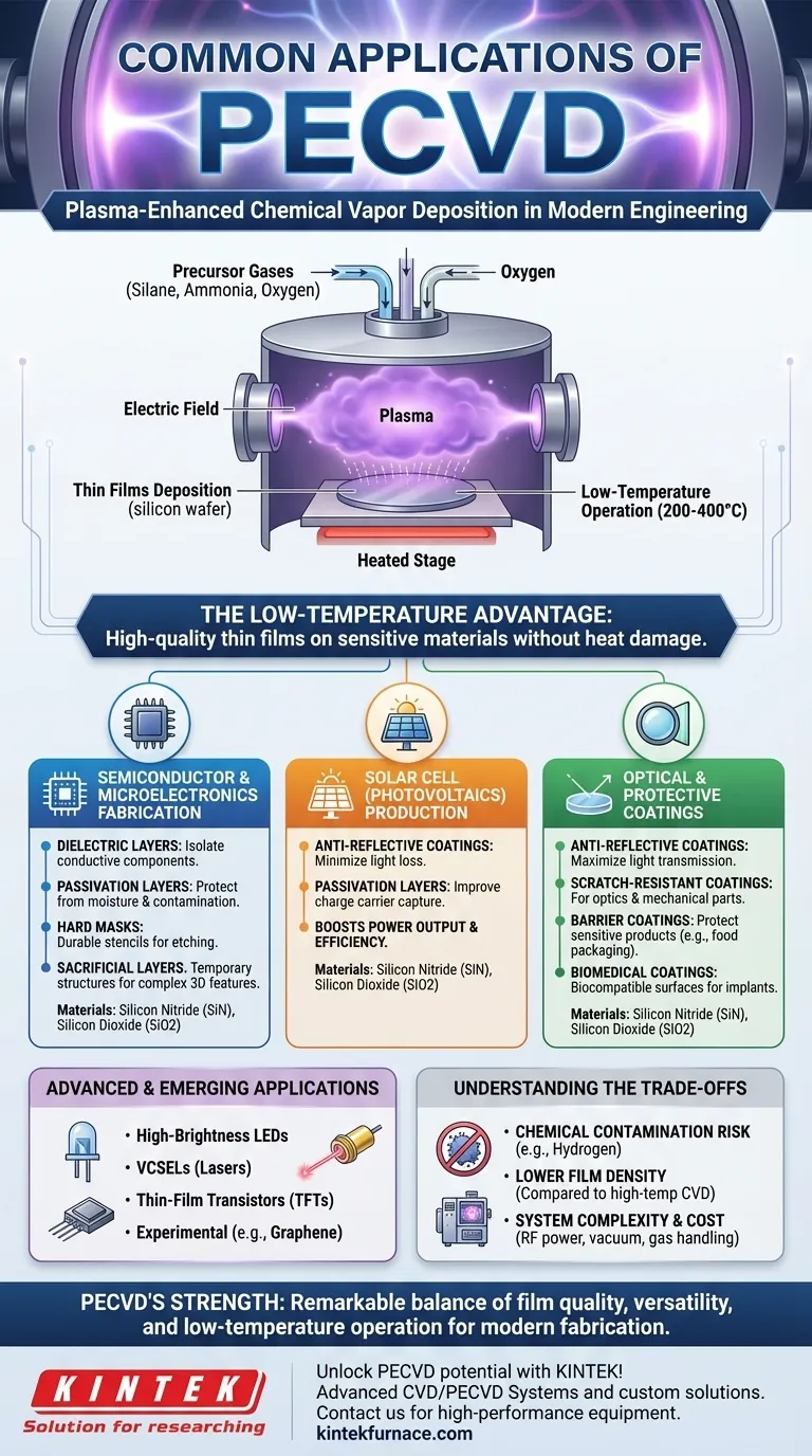
In modern engineering, one of the most common and critical applications of Plasma-Enhanced Chemical Vapor Deposition (PECVD) is in the semiconductor industry for fabricating integrated circuits. This process is essential for depositing thin dielectric films, such as silicon nitride and silicon dioxide, which act as insulators, protective layers, and masks on silicon wafers. Beyond semiconductors, PECVD is also a foundational technology in producing solar cells, optical coatings, and protective barriers on a vast range of materials.
At its core, PECVD's value comes from one primary advantage: its ability to deposit high-quality, functional thin films at significantly lower temperatures than other methods. This unlocks the ability to coat sensitive materials that would otherwise be damaged by high heat.
Why PECVD is a Foundational Technology
Traditional Chemical Vapor Deposition (CVD) relies on high temperatures (often >600°C) to drive the chemical reactions needed to form a film. PECVD revolutionizes this by using an electric field to create plasma, an energized gas state.
The Low-Temperature Advantage
The energy from the plasma, rather than thermal energy, drives the deposition reaction. This allows the process to run at much lower temperatures (typically 200-400°C).
This is critical for depositing films on substrates that cannot withstand high heat, such as fully or partially fabricated electronic devices, flexible polymers, and certain plastics.
Precision and Film Quality
PECVD systems provide exceptional control over the properties of the deposited film. By precisely managing gas flow, pressure, and plasma power, engineers can dictate the film's thickness, uniformity, and composition.
This results in high-quality, functional layers that are essential for the performance of modern electronic and optical components.
Versatility of Deposited Materials
The process is highly versatile and can be used to deposit a wide range of materials. The most common include:
- Silicon Nitride (SiN): Used as a passivation layer and a chemical barrier.
- Silicon Dioxide (SiO2): A fundamental dielectric (insulator) in microelectronics.
- Silicon Carbide (SiC): Valued for its hardness and stability in high-temperature applications.
Key Application Domains
The unique capabilities of PECVD make it indispensable across several high-tech industries. It is not a niche process but a widespread manufacturing tool.
Semiconductor and Microelectronics Fabrication
This is arguably the most significant application. In the creation of integrated circuits (chips) and Micro-Electro-Mechanical Systems (MEMS), PECVD is used to create:
- Dielectric Layers: To electrically isolate conductive components from each other.
- Passivation Layers: To protect the device surface from moisture and contamination.
- Hard Masks: Durable stencils used during the etching phases of fabrication.
- Sacrificial Layers: Temporary structures that are later removed to create complex 3D features.
Solar Cell (Photovoltaics) Production
To maximize the efficiency of a solar cell, you must ensure as much light as possible enters the cell and that the generated electrons are captured effectively.
PECVD is used to deposit both anti-reflective coatings on the surface to reduce light loss and passivation layers that improve the capture of charge carriers, boosting the cell's overall power output.
Optical and Protective Coatings
PECVD is used to apply functional films to a wide variety of surfaces. These include:
- Anti-Reflective Coatings: For glasses, lenses, and optical sensors to maximize light transmission.
- Scratch-Resistant Coatings: Hard, durable layers applied to optics like sunglasses or even mechanical components.
- Barrier Coatings: Dense, inert films that protect sensitive products. A common example is the ultra-thin barrier inside food packaging (like potato chip bags) that prevents moisture and oxygen from getting in.
- Biomedical Coatings: Used to create biocompatible or protective surfaces on medical implants.
Advanced and Emerging Applications
The utility of PECVD continues to expand into new fields. It is a key enabling technology for producing high-brightness LEDs, VCSELs (a type of laser), thin-film transistors (TFTs), and even for experimental work like depositing vertically aligned graphene.
Understanding the Trade-offs
While incredibly powerful, PECVD is not without its compromises. Understanding these is key to making an informed engineering decision.
Chemical Contamination Risk
Because the process uses precursor gases (like silane and ammonia), there is a risk that hydrogen and other atomic fragments from the plasma can be incorporated into the deposited film. This can sometimes affect the film's electrical or optical properties.
Film Density and Stoichiometry
Compared to high-temperature deposition methods like Low-Pressure CVD (LPCVD), films created by PECVD can sometimes be less dense and may not have a perfect chemical composition (stoichiometry). This is the direct trade-off for the benefit of low-temperature processing.
System Complexity and Cost
Generating and maintaining a stable plasma requires complex and expensive equipment, including RF power generators, vacuum systems, and sophisticated gas handling. This makes PECVD systems more complex than simple thermal reactors.
Making the Right Choice for Your Goal
Selecting a deposition method depends entirely on the requirements of your substrate and the desired film properties.
- If your primary focus is mass-producing silicon electronics: PECVD is the industry standard for depositing high-quality dielectrics without damaging previously fabricated layers.
- If your primary focus is coating heat-sensitive substrates like polymers: PECVD is often the only viable choice, as high-temperature methods would destroy the underlying material.
- If your primary focus is the absolute highest film purity and density: You should consider a higher-temperature process like LPCVD, but only if your substrate can tolerate the heat.
Ultimately, PECVD's strength lies in its remarkable balance of film quality, versatility, and low-temperature operation, making it a cornerstone of modern fabrication.
Summary Table:
| Application Domain | Key Uses | Key Materials Deposited |
|---|---|---|
| Semiconductor Fabrication | Dielectric layers, passivation, hard masks | Silicon Nitride (SiN), Silicon Dioxide (SiO2) |
| Solar Cell Production | Anti-reflective coatings, passivation layers | Silicon Nitride (SiN), Silicon Dioxide (SiO2) |
| Optical and Protective Coatings | Anti-reflective, scratch-resistant, barrier films | Silicon Nitride (SiN), Silicon Dioxide (SiO2) |
| Emerging Applications | LEDs, VCSELs, thin-film transistors | Silicon Carbide (SiC), others |
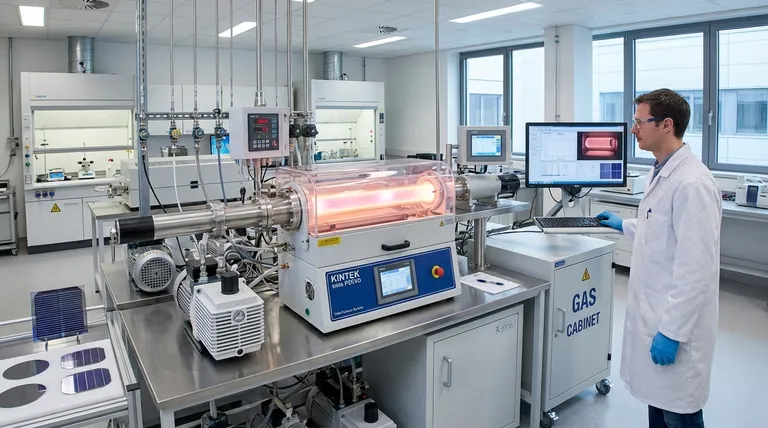
Unlock the full potential of PECVD for your laboratory with KINTEK! Leveraging exceptional R&D and in-house manufacturing, we provide advanced high-temperature furnace solutions tailored to your needs. Our product line includes Muffle, Tube, Rotary Furnaces, Vacuum & Atmosphere Furnaces, and CVD/PECVD Systems, complemented by strong deep customization capabilities to precisely meet unique experimental requirements. Whether you're in semiconductor, solar, or optical industries, KINTEK delivers reliable, high-performance equipment to enhance your research and production. Contact us today to discuss how we can support your projects with cutting-edge technology and expert solutions!
Visual Guide
Related Products
- Slide PECVD Tube Furnace with Liquid Gasifier PECVD Machine
- RF PECVD System Radio Frequency Plasma Enhanced Chemical Vapor Deposition
- Inclined Rotary Plasma Enhanced Chemical Deposition PECVD Tube Furnace Machine
- Inclined Rotary Plasma Enhanced Chemical Deposition PECVD Tube Furnace Machine
- Multi Heating Zones CVD Tube Furnace Machine for Chemical Vapor Deposition Equipment
People Also Ask
- In which industries is the tube furnace commonly used? Essential for Materials Science, Energy, and More
- What are the advantages of using a tube furnace CVD system for Cu(111)/graphene? Superior Scalability and Quality
- How does PECVD equipment contribute to TOPCon bottom cells? Mastering Hydrogenation for Maximum Solar Efficiency
- What are the main advantages of PECVD tube furnaces compared to CVD tube furnaces? Lower Temp, Faster Deposition, and More
- What are the disadvantages of tube furnace cracking when processing heavy raw materials? Avoid Costly Downtime and Inefficiency


