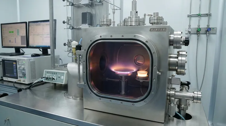
The in-situ combination of Plasma Enhanced Chemical Vapor Deposition (PECVD) and vacuum evaporation is essential because it prevents atmospheric exposure during the critical transition phases of fabrication. By housing both technologies within a single vacuum system, the process eliminates the risk of oxidation and contamination that occurs when moving samples between separate machines. This ensures the integrity of the interfaces between the germanium nanocrystals and the surrounding silicon carbide layers.
Core Takeaway Reliable nanocomposite integration relies on atomically pristine interfaces. By maintaining a continuous vacuum during the deposition of the base, nanolayer, and capping layer, you effectively avoid the formation of oxide barriers and contaminants, guaranteeing high-quality physical contact between the germanium nanocrystals and the silicon carbide matrix.
The Necessity of a Continuous Process
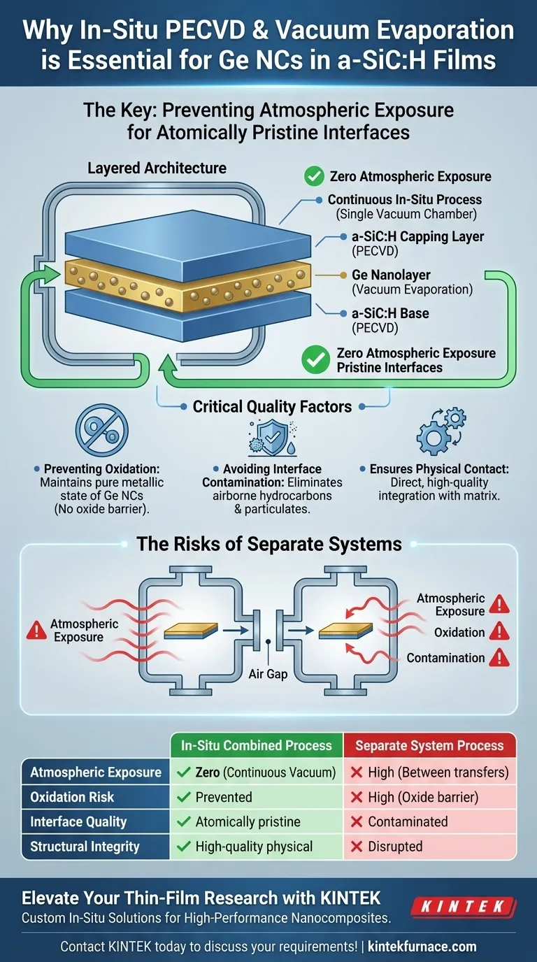
The Layered Architecture
The fabrication of these films involves a precise "sandwich" structure.
This consists of an a-SiC:H base, a central germanium nanolayer, and a final a-SiC:H capping layer.
Each layer requires a specific deposition technology—PECVD for the amorphous silicon carbide and vacuum evaporation for the germanium—making the transition between methods a critical point of failure.
Eliminating the Air Gap
In standard fabrication workflows, switching deposition methods often requires moving the sample from one chamber to another.
This transfer forces the sample to pass through the ambient atmosphere, exposing sensitive surfaces to air.
An in-situ system allows the operator to switch between PECVD and evaporation technologies without ever breaking the vacuum seal.
Critical Quality Factors
Preventing Oxidation
Germanium nanostructures are highly sensitive to oxygen.
Exposure to the atmosphere, even for a brief moment, can cause an oxide layer to form on the surface of the nanocrystals.
The single-chamber approach ensures the germanium remains in its pure metallic state before being sealed by the capping layer.
Avoiding Interface Contamination
Atmospheric exposure introduces unintended elements to the material interface.
These include airborne hydrocarbons, moisture, and microscopic particulates that settle on the surface.
Interface contamination acts as a barrier, disrupting the electrical and structural continuity of the film.
Ensuring Physical Contact
The performance of the final material depends on the interaction between the Ge nanocrystals and the a-SiC:H matrix.
Any foreign material or oxide layer creates a gap or insulation at this junction.
The in-situ process guarantees high-quality physical contact, allowing the nanocrystals to integrate directly with the matrix.
The Risks of Separate Systems
The "Contamination Penalty"
While utilizing separate machines for PECVD and evaporation might seem logistically simpler, it introduces a severe quality penalty.
The moment a sample leaves a vacuum environment, the surface energy changes and adsorption of impurities begins immediately.
Cleaning steps attempted after exposure are rarely sufficient to restore the surface to the pristine condition maintained by an in-situ process.
Making the Right Choice for Your Goal
To maximize the performance of germanium nanocrystals in silicon carbide films, consider the following regarding your equipment setup:
- If your primary focus is material purity: You must utilize an in-situ combined system to prevent the formation of insulating oxide layers at the crystal interfaces.
- If your primary focus is structural integrity: You should ensure the vacuum is maintained continuously between the base layer, the nanolayer, and the capping layer to guarantee direct physical contact.
By eliminating the variable of atmospheric exposure, you transform the interface from a point of failure into a foundation for high-quality device performance.
Summary Table:
| Feature | In-Situ Combined Process | Separate System Process |
|---|---|---|
| Atmospheric Exposure | Zero (Continuous Vacuum) | High (Between transfers) |
| Oxidation Risk | Prevented; pure metallic state | High; oxide barrier formation |
| Interface Quality | Atomically pristine contact | Contaminated by moisture/hydrocarbons |
| Structural Integrity | High-quality physical contact | Disrupted electrical continuity |
| Fabrication Efficiency | Seamless transition between layers | Requires cleaning and re-pumping |
Elevate Your Thin-Film Research with KINTEK
Achieving atomically pristine interfaces is critical for high-performance nanocomposites. Backed by expert R&D and manufacturing, KINTEK offers cutting-edge PECVD, Vacuum Evaporation, CVD systems, and other lab high-temp furnaces, all customizable for your unique material needs. Don't let atmospheric contamination compromise your Ge NCs integration. Our advanced in-situ solutions guarantee the structural integrity and purity your research demands.
Contact KINTEK today to discuss your custom furnace and deposition requirements!
Visual Guide
References
- Z. Remeš, Oleg Babčenko. Thin Hydrogenated Amorphous Silicon Carbide Layers with Embedded Ge Nanocrystals. DOI: 10.3390/nano15030176
This article is also based on technical information from Kintek Furnace Knowledge Base .
Related Products
- RF PECVD System Radio Frequency Plasma Enhanced Chemical Vapor Deposition
- Slide PECVD Tube Furnace with Liquid Gasifier PECVD Machine
- Inclined Rotary Plasma Enhanced Chemical Deposition PECVD Tube Furnace Machine
- Inclined Rotary Plasma Enhanced Chemical Deposition PECVD Tube Furnace Machine
- MPCVD Machine System Reactor Bell-jar Resonator for Lab and Diamond Growth
People Also Ask
- What is RF in PECVD? A Critical Control for Plasma Deposition
- What are the limitations of PECVD? Overcome Process Control and Cost Challenges
- How are deposition rates and film properties controlled in PECVD? Master Key Parameters for Optimal Thin Films
- What are the system specifications of the PECVD system? Unlock Precision Thin-Film Deposition
- What are the key advantages of PECVD technology? Achieve Low-Temperature, High-Quality Thin Film Deposition


