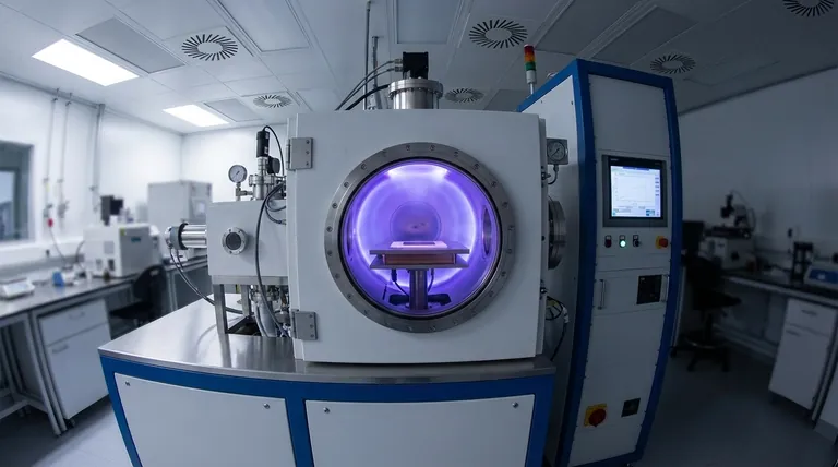
Plasma vapor deposition, more accurately known as Plasma-Enhanced Chemical Vapor Deposition (PECVD), is a process that uses an energized gas, or plasma, to deposit ultra-thin films of material onto a substrate's surface. Unlike traditional deposition methods that rely on high heat, PECVD uses the energy of the plasma to drive the necessary chemical reactions. This allows the process to run at much lower temperatures, making it a highly versatile and efficient technique for creating advanced materials like synthetic diamond coatings.
The fundamental advantage of plasma vapor deposition is its use of plasma to energize precursor gases. This activation allows high-quality thin films to be formed at significantly lower temperatures than conventional methods, broadening the range of materials and substrates that can be used.
The Critical Role of Plasma
To understand PECVD, one must first appreciate why plasma is a game-changer compared to conventional Chemical Vapor Deposition (CVD).
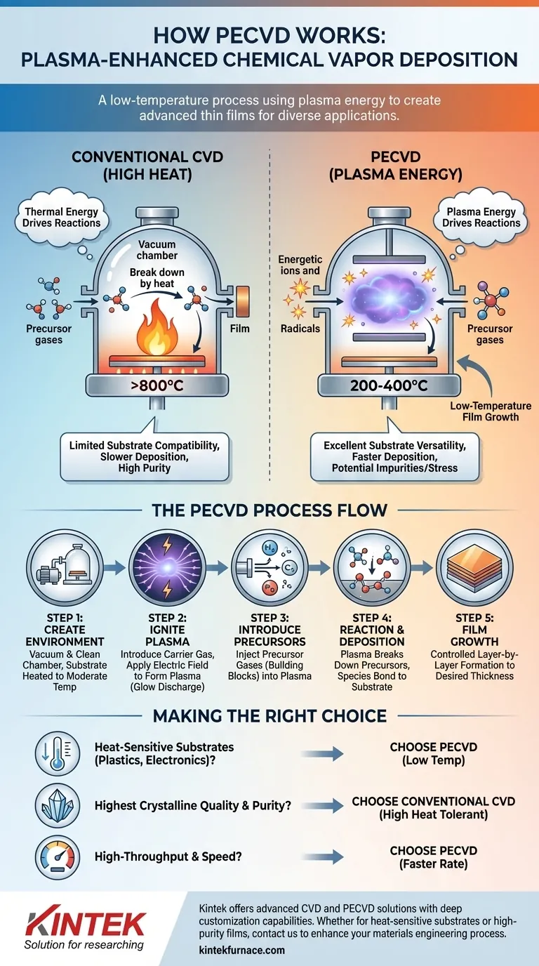
Breaking Down Conventional CVD
Traditional CVD works by heating a substrate in a vacuum chamber and introducing precursor gases. The intense heat (often >800°C) breaks the chemical bonds in the gas molecules, which then deposit onto the hot surface atom-by-atom to form a solid film.
The Plasma Advantage: Energy Without Heat
PECVD achieves the same outcome but replaces most of the thermal energy with electrical energy. By applying a strong electric field (often from a microwave source) to a gas at low pressure, the gas becomes ionized and forms a plasma—an energized state of matter.
This plasma contains highly reactive ions and free radicals. When precursor gases are introduced, the plasma's energy—not extreme heat—is what breaks them down into the building blocks needed for the film. This allows the substrate to remain at a much lower temperature (e.g., 200-400°C).
The Step-by-Step PECVD Process
The deposition process is a highly controlled sequence of events that takes place inside a vacuum chamber.
Step 1: Creating the Environment
First, a vacuum is created in the reaction chamber to remove any contaminants. The substrate, which is the object to be coated, is placed inside and often heated to a specific, moderate temperature to promote film adhesion.
Step 2: Plasma Ignition
A carrier gas (like argon or hydrogen) is introduced into the chamber at low pressure. An electric field is then applied, stripping electrons from the gas atoms and igniting the plasma. This is often visible as a characteristic glow, known as a glow discharge.
Step 3: Introducing Precursor Gases
With the plasma stable, the chemical precursor gases are introduced. These are the "ingredients" that contain the atoms required to build the final film (e.g., silane gas to create a silicon film).
Step 4: Reaction and Deposition
The high-energy plasma immediately bombards the precursor gas molecules, breaking them into highly reactive chemical species. These reactive fragments then travel to the substrate's surface, where they bond and arrange themselves into a solid, thin film.
Step 5: Film Growth
This process continues layer by layer, allowing for precise control over the film's thickness, from a few nanometers up to several micrometers.
Understanding the Trade-offs
While powerful, PECVD is not a universal solution. It involves a clear set of trade-offs compared to traditional high-temperature CVD.
Advantage: Substrate Versatility
The most significant benefit of PECVD is its low operating temperature. This makes it possible to coat heat-sensitive materials, such as plastics, polymers, and complex electronic devices, that would be damaged or destroyed by the heat of conventional CVD.
Advantage: Faster Deposition
The highly reactive plasma environment can often lead to significantly faster film growth compared to purely thermal processes, making PECVD more efficient for many manufacturing applications.
Potential Drawback: Film Purity
The energetic and complex chemical environment of the plasma can sometimes lead to the incorporation of impurities (like hydrogen from a carrier gas) into the film. This can affect material properties like density and electrical conductivity.
Potential Drawback: Internal Stress
Films grown via PECVD can sometimes have higher internal stress due to the ion bombardment during deposition. In contrast, slower, high-temperature CVD can produce more stable, crystalline structures with lower stress.
Making the Right Choice for Your Goal
Selecting the correct deposition method requires matching the process capabilities to the final application's requirements.
- If your primary focus is coating heat-sensitive substrates: PECVD is the definitive choice due to its low-temperature operation.
- If your primary focus is achieving the highest possible crystalline quality and purity: Conventional CVD may be superior, assuming your substrate can tolerate the extreme heat.
- If your primary focus is high-throughput manufacturing and speed: PECVD's faster deposition rates often provide a significant economic and operational advantage.
By understanding that plasma's role is to provide energy without heat, you can effectively leverage PECVD to engineer advanced materials for a new generation of products.
Summary Table:
| Aspect | Plasma-Enhanced CVD (PECVD) | Conventional CVD |
|---|---|---|
| Process Temperature | Low (200-400°C) | High (>800°C) |
| Primary Energy Source | Electrical (Plasma) | Thermal (Heat) |
| Substrate Compatibility | Excellent for heat-sensitive materials (plastics, electronics) | Limited to high-temperature tolerant materials |
| Deposition Speed | Faster | Slower |
| Film Purity | Potential for impurities (e.g., hydrogen) | Typically higher purity |
| Film Stress | Can have higher internal stress | Lower stress, more stable crystalline structures |
Need a precise thin-film deposition solution for your unique requirements?
At KINTEK, we leverage our exceptional R&D and in-house manufacturing capabilities to provide advanced high-temperature furnace solutions, including specialized CVD and PECVD systems. Our product line is complemented by strong deep customization capabilities to precisely meet your unique experimental and production needs.
Whether you're working with heat-sensitive substrates or require high-purity films, our experts can help you select or customize the ideal system for your application.
Contact us today to discuss how our PECVD and furnace solutions can enhance your materials engineering process!
Visual Guide
Related Products
- RF PECVD System Radio Frequency Plasma Enhanced Chemical Vapor Deposition
- Slide PECVD Tube Furnace with Liquid Gasifier PECVD Machine
- Inclined Rotary Plasma Enhanced Chemical Deposition PECVD Tube Furnace Machine
- Inclined Rotary Plasma Enhanced Chemical Deposition PECVD Tube Furnace Machine
- 915MHz MPCVD Diamond Machine Microwave Plasma Chemical Vapor Deposition System Reactor
People Also Ask
- What are the applications of plasma enhanced chemical vapor deposition? Key Uses in Electronics, Optics & Materials
- What are some promising applications of PECVD-prepared 2D materials? Unlock Advanced Sensing and Optoelectronics
- How does film quality compare between PECVD and CVD? Choose the Best Method for Your Substrate
- How is silicon dioxide deposited from tetraethylorthosilicate (TEOS) in PECVD? Achieve Low-Temperature, High-Quality SiO2 Films
- How are deposition rates and film properties controlled in PECVD? Master Key Parameters for Optimal Thin Films


