In essence, Plasma-Enhanced Chemical Vapor Deposition (PECVD) overcomes the primary limitation of conventional thermal CVD by using an energy-rich plasma to drive chemical reactions instead of high heat. This fundamental difference allows for the deposition of high-quality, high-purity thin films at significantly lower temperatures, making it a cornerstone technology for modern electronics and advanced materials.
PECVD's central advantage is its ability to decouple deposition temperature from film quality. It achieves results at low temperatures (200-400°C) that would otherwise require extreme heat, unlocking high-performance film deposition on sensitive substrates that traditional methods would damage or destroy.
The Core Advantage: Decoupling Temperature and Quality
The power of PECVD lies in its use of plasma—an ionized gas containing a mix of ions, electrons, and neutral species. This plasma provides the energy for chemical reactions to occur on a substrate surface, replacing the need for high thermal energy.
Low-Temperature Processing
Traditional Chemical Vapor Deposition (CVD) often requires temperatures exceeding 600°C, which can damage or warp temperature-sensitive materials like polymers, plastics, or complex integrated circuits with pre-existing layers.
PECVD operates at much lower temperatures, typically between 200-400°C, and sometimes even at room temperature. This capability is indispensable for fabricating advanced semiconductors, flexible electronics, and medical devices.
Plasma-Enhanced Reaction Rates
The highly reactive species within the plasma dramatically accelerate the chemical reactions needed for film growth. This allows PECVD to achieve deposition rates that can be orders of magnitude faster than conventional CVD for certain materials.
This increased efficiency reduces process time, lowers energy consumption, and ultimately decreases manufacturing costs while increasing throughput.
Superior Film Characteristics
The unique deposition environment created by the plasma results in films with properties that are often superior to those produced by other methods.
High Purity, Density, and Low Stress
The plasma process promotes the formation of dense, high-purity films with fewer pinhole defects.
Furthermore, the low processing temperature minimizes thermal stress between the deposited film and the substrate, which is critical for preventing cracking and delamination, especially when materials have different thermal expansion coefficients.
Excellent Adhesion and Coverage
PECVD provides exceptional adhesion of the film to the substrate. The plasma can effectively clean and activate the substrate surface just before deposition, creating a stronger bond.
It also offers excellent, uniform step coverage, meaning it can evenly coat complex, three-dimensional surfaces and fill deep trenches without creating voids. This is crucial for the intricate topographies of microelectronic devices.
Enhanced Chemical and Thermal Stability
Films deposited via PECVD, such as silicon nitride or silicon dioxide, exhibit outstanding chemical and corrosion resistance. This makes them ideal for creating protective, encapsulating layers that shield sensitive components from the environment.
Understanding the Trade-offs
While powerful, PECVD is not without its complexities. Acknowledging its limitations is key to using it effectively.
Process Complexity
A PECVD system has more process variables to control than a simple thermal CVD reactor. Managing plasma power, frequency, pressure, and gas flow rates requires sophisticated control systems and a deeper process understanding to achieve repeatable results.
Precursor Chemistry
The quality of a PECVD film is highly dependent on the purity and type of precursor gases used. These gases can be complex, expensive, or hazardous, adding to the overall cost and safety considerations of the process.
Potential for Plasma-Induced Damage
While the plasma enables low-temperature deposition, its high-energy ions can sometimes cause physical or electrical damage to the substrate surface or the growing film. This risk must be carefully managed by fine-tuning plasma parameters, especially when working with ultra-sensitive electronic materials.
Making the Right Choice for Your Application
Selecting PECVD depends entirely on the technical requirements of your film and the constraints of your substrate.
- If your primary focus is processing temperature-sensitive materials: PECVD is the definitive choice, as it protects underlying layers and substrates that cannot withstand high heat.
- If your primary focus is achieving high throughput: PECVD's rapid deposition rates make it a highly efficient manufacturing solution for many common films like silicon nitride and oxide.
- If your primary focus is creating durable, conformal coatings: PECVD excels at producing dense, pinhole-free films with excellent adhesion and coverage over complex topographies.
- If your primary focus is film property customization: The ability to tune film stress, refractive index, and other characteristics by adjusting plasma parameters gives PECVD unmatched versatility.
By leveraging plasma, PECVD provides an unparalleled combination of low-temperature operation, high-quality results, and process flexibility, securing its role as an essential tool in advanced manufacturing.
Summary Table:
| Advantage | Key Benefit |
|---|---|
| Low-Temperature Processing | Enables deposition on sensitive substrates (e.g., polymers, ICs) without damage |
| Plasma-Enhanced Reaction Rates | Accelerates deposition, increasing throughput and reducing costs |
| Superior Film Characteristics | Delivers high purity, density, adhesion, and conformal coverage |
| Process Flexibility | Allows tuning of film properties like stress and refractive index |
Ready to elevate your lab's capabilities with advanced PECVD solutions? KINTEK leverages exceptional R&D and in-house manufacturing to provide diverse laboratories with high-temperature furnace systems, including our specialized CVD/PECVD Systems. With strong deep customization, we precisely meet your unique experimental needs for low-temperature, high-quality thin film deposition. Contact us today to discuss how our tailored solutions can drive your innovations forward!
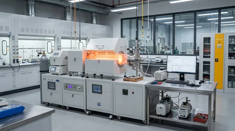
Visual Guide

Related Products
- Slide PECVD Tube Furnace with Liquid Gasifier PECVD Machine
- RF PECVD System Radio Frequency Plasma Enhanced Chemical Vapor Deposition
- Inclined Rotary Plasma Enhanced Chemical Deposition PECVD Tube Furnace Machine
- Inclined Rotary Plasma Enhanced Chemical Deposition PECVD Tube Furnace Machine
- Multi Heating Zones CVD Tube Furnace Machine for Chemical Vapor Deposition Equipment
People Also Ask
- What plasma source is used in PE-CVD tube furnaces? Unlock Low-Temperature, High-Quality Deposition
- What are the typical conditions for plasma-enhanced CVD processes? Achieve Low-Temperature Thin Film Deposition
- What are the disadvantages of tube furnace cracking when processing heavy raw materials? Avoid Costly Downtime and Inefficiency
- What are the main advantages of PECVD tube furnaces compared to CVD tube furnaces? Lower Temp, Faster Deposition, and More
- How does a hydrogen reduction environment in an industrial tube furnace facilitate gold-copper alloy microspheres?


