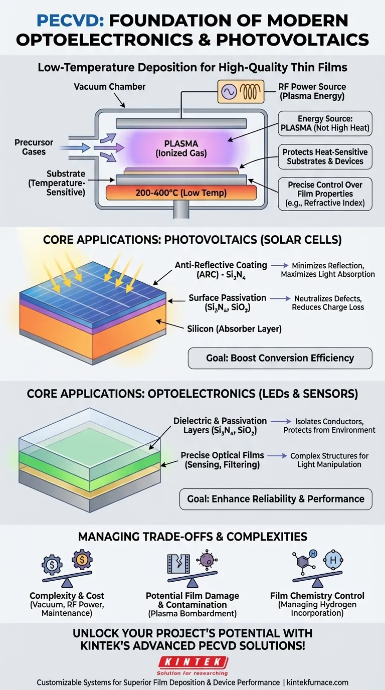
In essence, Plasma-Enhanced Chemical Vapor Deposition (PECVD) is a foundational manufacturing process for modern optoelectronics and photovoltaics. It enables the deposition of high-quality thin films at low temperatures, a critical requirement for creating efficient solar cells and reliable light-emitting diodes (LEDs) without damaging the heat-sensitive components underneath.
The core value of PECVD is its ability to decouple the energy required for a chemical reaction from thermal energy. By using an energized plasma instead of high heat, it allows for the growth of dense, uniform, and functional films on substrates that would otherwise be damaged or destroyed by traditional high-temperature methods.
Why PECVD is Essential for Advanced Devices
The key to PECVD's importance lies in its ability to overcome a fundamental manufacturing constraint: the need for high-quality materials on temperature-sensitive substrates.
The Low-Temperature Advantage
Traditional Chemical Vapor Deposition (CVD) requires very high temperatures (often >600°C) to provide the thermal energy needed for precursor gases to react and form a film.
These temperatures are destructive to many components used in photovoltaics and optoelectronics, such as the completed junctions of a silicon solar cell or the delicate quantum well structures in an LED.
PECVD solves this by using an electromagnetic field to create plasma, an ionized gas. This plasma provides the activation energy for the chemical reaction, allowing deposition to occur at much lower temperatures (typically 200-400°C).
Unmatched Control Over Film Properties
The plasma environment gives engineers precise control over the final film. By carefully managing process parameters like gas flow rates, pressure, and plasma power, they can meticulously tune the material's final properties.
This includes controlling the film's refractive index, density, chemical composition, and stress, all of which are critical for optical and electronic performance.
Core Applications in Photovoltaics (Solar Cells)
In photovoltaics, the goal is to convert as many photons as possible into electrons. PECVD is instrumental in depositing layers that directly improve this conversion efficiency.
Anti-Reflective Coatings (ARC)
A bare silicon surface reflects over 30% of incoming sunlight. An anti-reflective coating is a transparent layer with a precisely controlled thickness and refractive index that minimizes this reflection, allowing more light to enter the solar cell.
PECVD is the industry standard for depositing silicon nitride (Si₃N₄) films for this purpose. The process allows for precise tuning of the refractive index to maximize light absorption across the solar spectrum.
Surface Passivation
A major source of efficiency loss in a solar cell is "surface recombination," where charge carriers (electrons and holes) are lost at the silicon surface before they can be collected.
A passivation layer is an electrically insulating film that neutralizes these defects. The same silicon nitride film used for ARC also provides excellent surface passivation, serving a crucial dual role. **Silicon dioxide (SiO₂) is another common passivation film deposited via PECVD.
Core Applications in Optoelectronics (LEDs & Sensors)
Optoelectronic devices like LEDs and optical sensors also rely on complex, multi-layered structures that are sensitive to heat.
Dielectric and Passivation Layers
LEDs require high-quality insulating layers (dielectrics) to isolate different conductive parts of the device and prevent short circuits. They also need passivation layers to protect the sensitive semiconductor material from environmental degradation, ensuring long-term reliability and stable light output.
PECVD's ability to deposit dense, pinhole-free films of Si₃N₄ and SiO₂ at low temperatures is vital for manufacturing robust and long-lasting LEDs.
Precise Optical Films
For optical sensors, photometers, and data storage systems, PECVD is used to create a wide array of optical coatings. The precise control over the refractive index allows for the fabrication of complex filters, waveguides, and other structures that manipulate light in specific ways.
Understanding the Trade-offs
While powerful, PECVD is not a universal solution. It involves specific complexities that must be managed.
Complexity and Cost
PECVD systems are inherently more complex than thermal CVD reactors. They require vacuum chambers, gas handling systems, and sophisticated radio-frequency (RF) or microwave power sources to generate the plasma, leading to higher equipment and maintenance costs.
Potential for Film Damage and Contamination
While the ions in the plasma drive the chemical reaction, they can also physically bombard the substrate. If not properly controlled, this can introduce defects or damage into the growing film or the underlying device. The process is also sensitive to contamination from the chamber walls or precursor gases.
Control of Film Chemistry
The plasma environment is highly reactive and can lead to the incorporation of other elements, such as hydrogen, into the film. While sometimes desirable (as in amorphous silicon), this can also alter the intended film properties and must be carefully controlled.
How to Apply This to Your Goal
The decision to use PECVD is driven by the trade-off between device performance requirements and manufacturing constraints.
- If your primary focus is maximizing solar cell efficiency: You must use PECVD to deposit high-quality, dual-function silicon nitride films for anti-reflection and surface passivation.
- If your primary focus is manufacturing reliable, high-performance LEDs: Rely on PECVD to deposit robust passivation and dielectric films without damaging the light-emitting layers.
- If your primary focus is cost-sensitive applications with high-temperature tolerance: Simpler methods like atmospheric pressure CVD or sputtering may be more economical if the substrate can withstand the heat.
Ultimately, PECVD empowers engineers to build higher-performing devices by depositing superior films under conditions that would otherwise be impossible.
Summary Table:
| Application Area | Key Uses of PECVD | Benefits |
|---|---|---|
| Photovoltaics | Anti-reflective coatings, surface passivation | Increases light absorption, reduces charge carrier loss |
| Optoelectronics | Dielectric layers, passivation, optical films | Enhances device reliability, precise light manipulation |
| General | Low-temperature deposition | Protects heat-sensitive substrates, enables complex structures |
Unlock the full potential of your optoelectronic and photovoltaic projects with KINTEK's advanced PECVD solutions! Leveraging exceptional R&D and in-house manufacturing, we offer a range of high-temperature furnaces, including CVD/PECVD Systems, tailored to your unique needs. Our deep customization capabilities ensure precise film deposition for superior device performance. Contact us today to discuss how we can enhance your lab's efficiency and innovation!
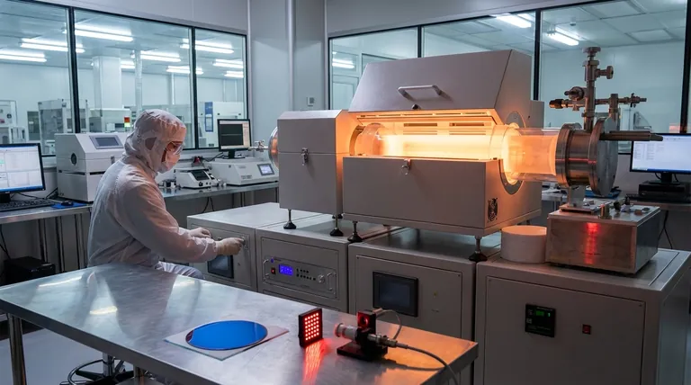
Visual Guide
Related Products
- RF PECVD System Radio Frequency Plasma Enhanced Chemical Vapor Deposition
- Slide PECVD Tube Furnace with Liquid Gasifier PECVD Machine
- Inclined Rotary Plasma Enhanced Chemical Deposition PECVD Tube Furnace Machine
- Inclined Rotary Plasma Enhanced Chemical Deposition PECVD Tube Furnace Machine
- Cylindrical Resonator MPCVD Machine System for Lab Diamond Growth
People Also Ask
- What are the applications of plasma enhanced chemical vapor deposition? Key Uses in Electronics, Optics & Materials
- How does film quality compare between PECVD and CVD? Choose the Best Method for Your Substrate
- What are the advantages of PECVD in film deposition? Achieve Low-Temp, High-Quality Coatings
- What is the role of RF power in PECVD and how does the RF-PECVD process work? Master Thin Film Deposition Control
- What is PECVD specification? A Guide to Choosing the Right System for Your Lab


