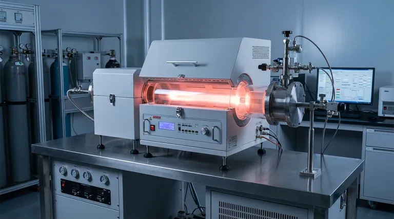
At its core, Plasma-Enhanced Chemical Vapor Deposition (PECVD) equipment works by using an electric field to create a plasma inside a vacuum chamber. This plasma energizes precursor gases, breaking them down into reactive components. These components then settle on a substrate, forming a solid thin film at temperatures significantly lower than those required by conventional deposition methods.
The fundamental purpose of using plasma in PECVD is to replace high thermal energy with electrical energy. This allows high-quality thin films to be grown at low temperatures, enabling deposition on substrates that cannot withstand intense heat.
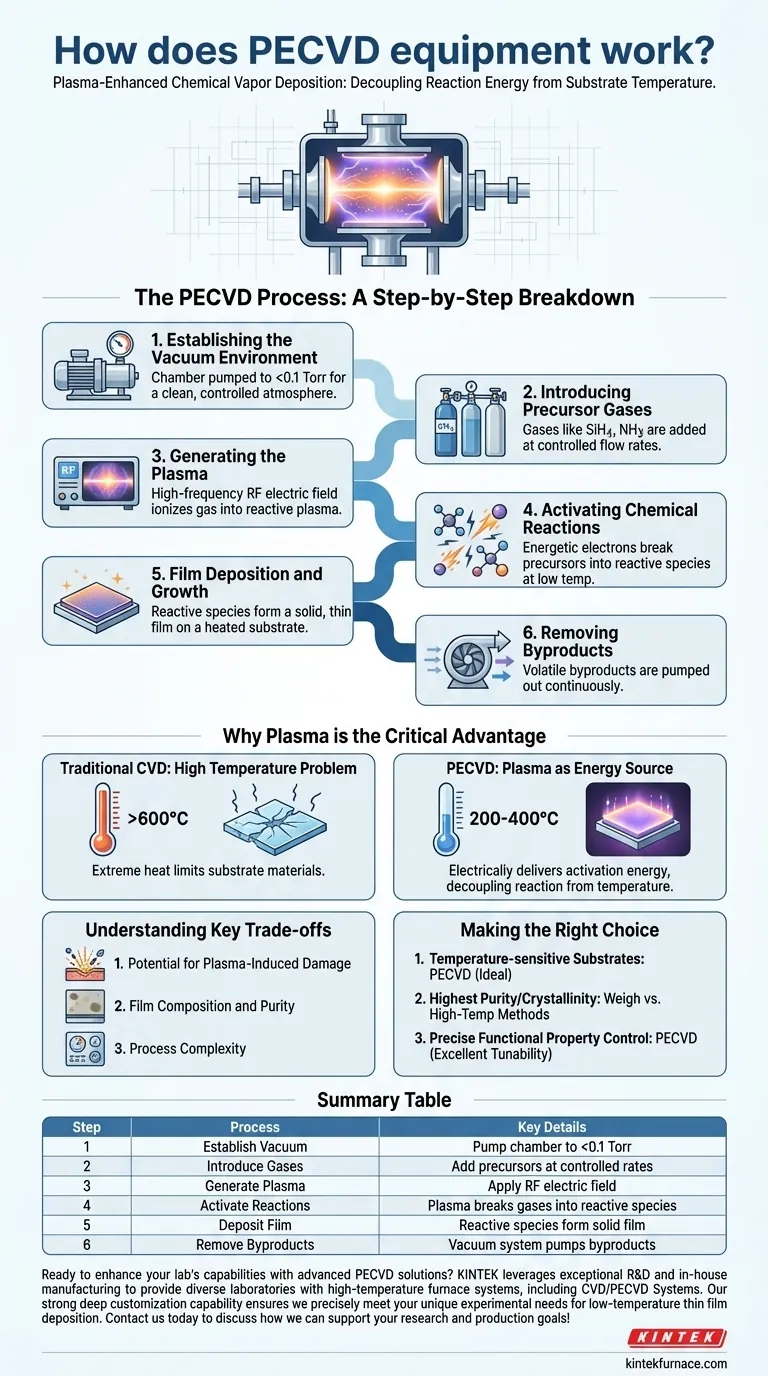
The PECVD Process: A Step-by-Step Breakdown
To understand how PECVD equipment functions, it is best to view it as a sequence of controlled events occurring within a highly engineered environment.
Step 1: Establishing the Vacuum Environment
The entire process takes place inside a sealed vacuum chamber. A pumping system reduces the pressure to a low level (typically below 0.1 Torr), removing contaminants and giving operators precise control over the atmosphere.
Step 2: Introducing Precursor Gases
Specific precursor gases, such as silane (SiH4) or ammonia (NH3), are introduced into the chamber at controlled flow rates. These gases contain the atoms required to build the desired film material.
Step 3: Generating the Plasma
A high-frequency electric field (Radio Frequency or RF) is applied between two electrodes inside the chamber. This powerful field strips electrons from the gas molecules, creating a glowing, ionized gas known as a plasma.
Step 4: Activating Chemical Reactions
Within the plasma, energetic electrons (with energies of 100-300 eV) collide with the neutral precursor gas molecules. These collisions transfer energy, breaking the molecules apart into highly reactive species, including ions and radicals, without significantly heating the entire chamber.
Step 5: Film Deposition and Growth
These newly formed reactive species diffuse through the chamber and land on the substrate, which is often gently heated to a specific, controlled temperature. They then chemically adsorb to the surface, react with each other, and build up the solid thin film layer by layer.
Step 6: Removing Byproducts
The chemical reactions on the substrate surface often create volatile byproducts. The chamber's vacuum system continuously pumps these byproducts away, ensuring a clean deposition process.
Why Plasma is the Critical Advantage
The "plasma-enhanced" aspect of PECVD is not just a detail; it is the central feature that provides its most significant benefits over other methods like traditional Chemical Vapor Deposition (CVD).
The Problem with High Temperature
Traditional CVD relies solely on high temperatures (often >600°C) to provide the thermal energy needed to break chemical bonds and initiate film-forming reactions. This extreme heat prevents its use on substrates like plastics, certain semiconductors, or other materials that would melt or be damaged.
Plasma as an Energy Source
PECVD solves this problem by using the plasma as the primary energy source. It delivers the activation energy required for chemical reactions electrically, not thermally. This masterfully decouples the reaction energy from the substrate temperature, allowing for deposition at much lower temperatures (typically 200-400°C).
Precise Control Over Film Properties
Because the plasma energy can be controlled independently from temperature, operators gain immense control. By adjusting parameters like RF power, gas pressure, and gas flow rates, they can finely tune critical film properties such as refractive index, material stress, electrical characteristics, and density.
Understanding the Key Trade-offs
While powerful, the PECVD process involves inherent compromises that are critical to understand for any application.
Potential for Plasma-Induced Damage
The same high-energy ions that enable low-temperature deposition can also bombard the substrate surface. This bombardment can sometimes cause physical or electrical damage, a crucial consideration when working with delicate electronic devices.
Film Composition and Purity
Because the process runs at lower temperatures, reactions may not go to completion as cleanly as in high-temperature methods. This can lead to the incorporation of unwanted elements, such as hydrogen from precursor gases, into the final film, potentially affecting its purity and performance.
Process Complexity
Managing the physics of a plasma adds a significant layer of complexity. The interplay between pressure, power, gas chemistry, and chamber geometry requires sophisticated control systems and deep process knowledge to achieve consistent, high-quality results.
Making the Right Choice for Your Application
Selecting a deposition method depends entirely on the technical goals of your project.
- If your primary focus is depositing on temperature-sensitive substrates: PECVD is the ideal choice because it decouples the reaction energy from the substrate temperature, preventing thermal damage.
- If your primary focus is achieving the highest possible film purity or crystallinity: You must carefully weigh PECVD against higher-temperature methods, as plasma processes can introduce impurities or a more amorphous film structure.
- If your primary focus is precise control over functional film properties like stress or refractive index: PECVD offers excellent tunability by allowing you to adjust plasma parameters independently of substrate temperature.
Ultimately, understanding PECVD is about recognizing its power to use electrical energy to overcome the thermal limitations of traditional material deposition.
Summary Table:
| Step | Process | Key Details |
|---|---|---|
| 1 | Establish Vacuum | Pump chamber to <0.1 Torr for clean, controlled environment |
| 2 | Introduce Gases | Add precursors like SiH4 or NH3 at controlled flow rates |
| 3 | Generate Plasma | Apply RF electric field to create ionized gas plasma |
| 4 | Activate Reactions | Plasma breaks gases into reactive species at low temperatures |
| 5 | Deposit Film | Reactive species form solid thin film on substrate |
| 6 | Remove Byproducts | Vacuum system pumps out volatile byproducts |
Ready to enhance your lab's capabilities with advanced PECVD solutions? KINTEK leverages exceptional R&D and in-house manufacturing to provide diverse laboratories with high-temperature furnace systems, including CVD/PECVD Systems. Our strong deep customization capability ensures we precisely meet your unique experimental needs for low-temperature thin film deposition. Contact us today to discuss how we can support your research and production goals!
Visual Guide
Related Products
- Slide PECVD Tube Furnace with Liquid Gasifier PECVD Machine
- Inclined Rotary Plasma Enhanced Chemical Deposition PECVD Tube Furnace Machine
- Inclined Rotary Plasma Enhanced Chemical Deposition PECVD Tube Furnace Machine
- RF PECVD System Radio Frequency Plasma Enhanced Chemical Vapor Deposition
- Multi Heating Zones CVD Tube Furnace Machine for Chemical Vapor Deposition Equipment
People Also Ask
- In which industries is the tube furnace commonly used? Essential for Materials Science, Energy, and More
- How does a hydrogen reduction environment in an industrial tube furnace facilitate gold-copper alloy microspheres?
- What are the typical conditions for plasma-enhanced CVD processes? Achieve Low-Temperature Thin Film Deposition
- What are the disadvantages of tube furnace cracking when processing heavy raw materials? Avoid Costly Downtime and Inefficiency
- What plasma source is used in PE-CVD tube furnaces? Unlock Low-Temperature, High-Quality Deposition


