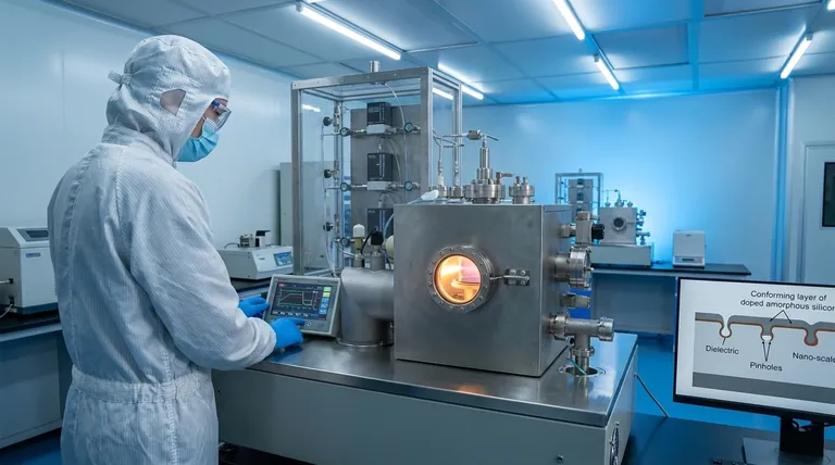
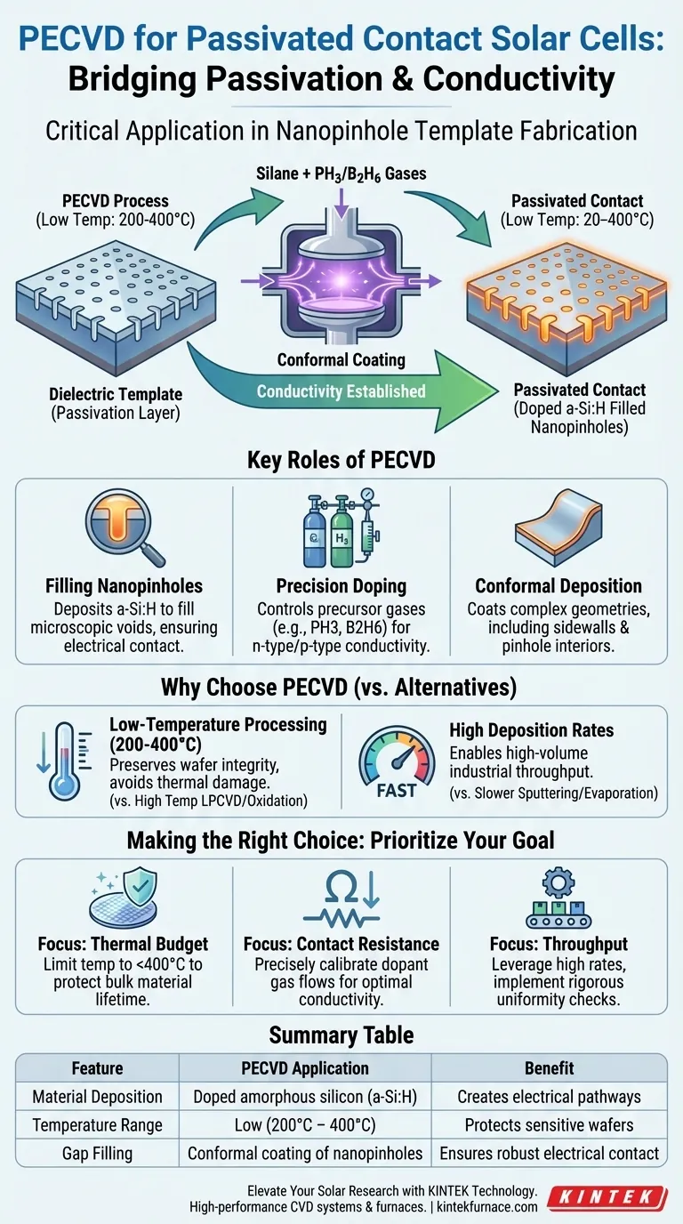
The critical application of Plasma Enhanced Chemical Vapor Deposition (PECVD) equipment in passivated contact fabrication is the deposition of doped amorphous silicon (a-Si:H) layers onto dielectric templates containing nanopinholes. This process is essential for filling these microscopic voids and coating the surface to establish the necessary electrical conductivity for the solar cell's passivated contact.
PECVD acts as the bridge between passivation and conductivity. It allows manufacturers to fill dielectric nanopinholes with doped silicon at lower thermal budgets (200–400°C), preserving the integrity of temperature-sensitive wafer structures while ensuring robust electrical contact.
The Role of PECVD in Contact Formation
Filling the Nanopinhole Template
The primary function of the PECVD system in this specific application is to deposit material onto a dielectric layer that acts as a mask. This dielectric layer features nanopinholes—tiny openings intended to allow electrical current to flow. The PECVD equipment must ensure that the deposited amorphous silicon effectively penetrates and fills these pinholes to contact the underlying wafer.
Precision Doping via Gas Control
To function as a passivated contact, the deposited silicon layer must be electrically conductive (doped). PECVD systems achieve this by strictly controlling the flow of precursor gases.
- Silane is used as the silicon source.
- Phosphine (PH3) or Diborane (B2H6) are introduced to dope the silicon n-type or p-type, respectively.
Conformal Film Deposition
Unlike line-of-sight deposition methods (such as evaporation), PECVD is capable of conformal coverage. This means it can coat complex geometries, including the sidewalls of structures and the interior of the nanopinholes. This capability is vital for ensuring a continuous, high-quality electrical pathway through the dielectric layer.
Why PECVD is Chosen Over Alternatives
Low-Temperature Processing
A defining advantage of PECVD is its ability to operate at relatively low temperatures, typically between 200°C and 400°C. High temperatures can damage certain wafer structures or degrade previously deposited layers. By using plasma energy rather than thermal energy to drive chemical reactions, PECVD avoids the high thermal budgets associated with Low Pressure Chemical Vapor Deposition (LPCVD) or thermal oxidation.
High Deposition Rates
In industrial manufacturing, throughput is critical. PECVD generally offers faster deposition rates compared to sputter deposition or thermal evaporation. This efficiency allows for high-volume production of solar cells without becoming a bottleneck in the fabrication line.
Understanding the Trade-offs
Uniformity vs. Speed
While PECVD is faster than many alternatives, this speed can sometimes come at the cost of film uniformity. Systems such as LPCVD often produce highly uniform polysilicon layers but require higher temperatures and longer processing times. Operators must carefully calibrate PECVD plasma parameters to minimize variations in film thickness across the wafer.
Material Quality and Defects
PECVD deposits amorphous silicon (a-Si), which has different electrical properties than crystalline silicon. While generally high quality with low roughness, the plasma process can occasionally induce surface defects if not managed correctly. However, for the specific application of creating passivated contacts via nanopinholes, the a-Si:H layer provides the necessary balance of passivation and conductivity.
Making the Right Choice for Your Goal
Depending on the specific requirements of your solar cell architecture, here is how to prioritize the application of PECVD:
- If your primary focus is Thermal Budget: Utilize PECVD to deposit essential contact layers without exposing the wafer to temperatures exceeding 400°C, preserving bulk material lifetime.
- If your primary focus is Contact Resistance: Prioritize the precise calibration of dopant gas flows (Phosphine/Diborane) to ensure the amorphous silicon filling the nanopinholes is sufficiently conductive.
- If your primary focus is Throughput: Leverage the high deposition rates of PECVD, but implement rigorous uniformity checks to ensure consistent performance across the entire solar module.
By mastering the gas flow ratios and plasma parameters, manufacturers can utilize PECVD to create high-efficiency passivated contacts that are both mechanically robust and electrically superior.
Summary Table:
| Feature | PECVD Application in Passivated Contacts | Benefit |
|---|---|---|
| Material Deposition | Doped amorphous silicon (a-Si:H) | Creates essential electrical pathways |
| Temperature Range | Low temperature (200°C – 400°C) | Protects temperature-sensitive wafers |
| Gap Filling | Conformal coating of nanopinholes | Ensures robust electrical contact |
| Doping Method | Precise precursor gas control (PH3/B2H6) | Customizes n-type or p-type conductivity |
| Production Speed | High deposition rates | Enables high-volume industrial throughput |
Elevate Your Solar Research with KINTEK Technology
Maximize your cell efficiency and thermal management with KINTEK’s advanced deposition solutions. Backed by expert R&D and world-class manufacturing, KINTEK offers high-performance CVD systems, Muffle, Tube, Rotary, and Vacuum furnaces, all fully customizable to meet your unique laboratory or industrial needs.
Whether you are optimizing nanopinhole templates or scaling up high-efficiency solar architectures, our team provides the precision tools necessary for superior material performance. Contact KINTEK today to discuss your custom furnace requirements and see how we can bring unparalleled value to your next project.
Visual Guide
References
- William Nemeth, Paul Stradins. Self‐Assembled Monolayer Templating for Engineered Nanopinholes in Passivated Contact Solar Cells. DOI: 10.1002/solr.202500200
This article is also based on technical information from Kintek Furnace Knowledge Base .
Related Products
- Slide PECVD Tube Furnace with Liquid Gasifier PECVD Machine
- RF PECVD System Radio Frequency Plasma Enhanced Chemical Vapor Deposition
- Inclined Rotary Plasma Enhanced Chemical Deposition PECVD Tube Furnace Machine
- Inclined Rotary Plasma Enhanced Chemical Deposition PECVD Tube Furnace Machine
- Cylindrical Resonator MPCVD Machine System for Lab Diamond Growth
People Also Ask
- In which industries is the tube furnace commonly used? Essential for Materials Science, Energy, and More
- What are the main advantages of PECVD tube furnaces compared to CVD tube furnaces? Lower Temp, Faster Deposition, and More
- What role does a Tube Furnace play in the CVD growth of carbon nanotubes? Achieve High-Purity CNT Synthesis
- What is plasma in the context of PECVD? Unlock Low-Temperature Thin Film Deposition
- What are the advantages of using a tube furnace CVD system for Cu(111)/graphene? Superior Scalability and Quality


