The primary purpose of Plasma-Enhanced Chemical Vapor Deposition (PECVD) is to deposit high-quality, durable thin films onto a substrate at significantly lower temperatures than traditional methods. It uses an energized plasma to drive the chemical reactions needed to form the film, making it an essential process for manufacturing modern electronics, optics, and advanced materials that cannot tolerate high heat.
PECVD overcomes the high-temperature limitations of conventional Chemical Vapor Deposition (CVD). By using plasma to energize precursor gases, it enables the creation of high-performance thin films on materials that would otherwise be damaged or destroyed by heat.
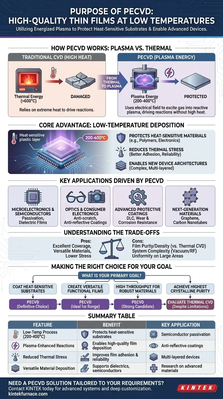
How PECVD Works: The Role of Plasma
From Thermal Energy to Plasma Energy
Traditional Chemical Vapor Deposition (CVD) relies on very high temperatures, often many hundreds of degrees Celsius, to provide the thermal energy needed to break down precursor gases and deposit a film.
PECVD fundamentally changes this equation. Instead of heat, it uses an electrical field to excite a gas into a plasma, an energetic state of matter containing ions, electrons, and free radicals.
Driving Reactions Without Extreme Heat
This plasma provides the energy required to initiate the chemical reactions. The highly reactive species in the plasma decompose the precursor gases and deposit the desired material onto the substrate surface, molecule by molecule.
Because the energy comes from the plasma rather than thermal agitation, the entire process can run at much lower temperatures, often between 200-400°C, and sometimes even lower.
The Core Advantage: Low-Temperature Deposition
Protecting Heat-Sensitive Substrates
The single most important benefit of PECVD is its ability to coat materials that cannot survive the high temperatures of conventional CVD.
This includes polymers, plastics, and fully assembled microelectronic devices with pre-existing sensitive components. Without PECVD, coating these materials would be impossible.
Reducing Material Stress
High temperatures create thermal stress in both the deposited film and the underlying substrate as they cool. This stress can lead to cracking, poor adhesion, and device failure.
By operating at lower temperatures, PECVD minimizes thermal stress, resulting in more durable and reliable films with excellent adhesion.
Enabling New Device Architectures
The ability to deposit high-quality dielectrics, semiconductors, and protective layers on a wide variety of substrates opens up new possibilities for engineers. It allows for the creation of complex, multi-layered devices that would otherwise be unmanufacturable.
Key Applications Driven by PECVD's Capabilities
Microelectronics and Semiconductors
PECVD is a cornerstone of the semiconductor industry. It is used to deposit critical layers such as passivation films that protect the chip surface, and insulating (dielectric) films that separate conductive layers.
Optics and Consumer Electronics
The hard, clear anti-scratch and anti-reflective coatings on eyeglasses, camera lenses, and smartphone screens are often created using PECVD. Its ability to coat surfaces evenly makes it ideal for these applications.
Advanced Protective Coatings
PECVD is used to deposit ultra-hard diamond-like carbon (DLC) films. These coatings provide exceptional wear and corrosion resistance for tools, automotive parts, and medical implants.
Next-Generation Materials
The process is also employed in cutting-edge research and development to synthesize advanced materials like graphene, carbon nanotubes, and even polycrystalline diamond films.
Understanding the Trade-offs
Film Purity and Density
While PECVD films are high-quality, the plasma environment can sometimes introduce hydrogen or other impurities into the film. For applications requiring the absolute highest purity or density, a higher-temperature thermal CVD process may still be necessary.
System Complexity
PECVD systems require vacuum chambers, gas handling, and radio-frequency (RF) or microwave power sources to generate the plasma. This makes them more complex and costly than some simpler, non-vacuum deposition techniques.
Deposition Uniformity
While PECVD provides excellent coverage over complex shapes, achieving perfect film thickness uniformity across very large substrates (like large-area displays or solar panels) requires careful reactor design and process control.
Making the Right Choice for Your Goal
When deciding if PECVD is the correct process, your primary goal is the most important factor.
- If your primary focus is coating heat-sensitive substrates: PECVD is the definitive choice, as its low-temperature process prevents damage to materials like plastics or integrated electronics.
- If your primary focus is creating versatile functional films: PECVD is ideal for its ability to deposit a wide range of materials, including insulators, protective layers, and semiconductors.
- If your primary focus is high throughput for robust materials: PECVD is often faster than low-pressure CVD, making it a strong candidate for efficient production.
- If your primary focus is achieving the absolute highest crystalline purity: You should evaluate whether a higher-temperature thermal CVD process is required for your specific material, despite its limitations.
Ultimately, PECVD is the definitive tool for engineering advanced surfaces on the vast range of materials that cannot withstand the heat of conventional methods.
Summary Table:
| Feature | Benefit | Key Application |
|---|---|---|
| Low-Temperature Process (200-400°C) | Protects heat-sensitive substrates like plastics & electronics | Semiconductor passivation, coating on polymers |
| Plasma-Enhanced Reactions | Enables high-quality film deposition without extreme heat | Anti-reflective coatings on lenses, DLC coatings |
| Reduced Thermal Stress | Improves film adhesion and device reliability | Multi-layered microelectronic devices |
| Versatile Material Deposition | Supports dielectrics, semiconductors, and protective films | Research on graphene, carbon nanotubes |
Need a PECVD solution tailored to your unique requirements?
At KINTEK, we leverage our exceptional R&D and in-house manufacturing to provide advanced PECVD systems and other high-temperature furnace solutions. Whether you're working in semiconductors, optics, or advanced materials research, our deep customization capabilities ensure your PECVD process meets your exact experimental and production goals.
Contact our experts today to discuss how our PECVD and CVD systems can enhance your lab's capabilities and drive your innovations forward.
Visual Guide
Related Products
- Slide PECVD Tube Furnace with Liquid Gasifier PECVD Machine
- RF PECVD System Radio Frequency Plasma Enhanced Chemical Vapor Deposition
- Inclined Rotary Plasma Enhanced Chemical Deposition PECVD Tube Furnace Machine
- Inclined Rotary Plasma Enhanced Chemical Deposition PECVD Tube Furnace Machine
- Multi Heating Zones CVD Tube Furnace Machine for Chemical Vapor Deposition Equipment
People Also Ask
- How does a hydrogen reduction environment in an industrial tube furnace facilitate gold-copper alloy microspheres?
- How does PECVD equipment contribute to TOPCon bottom cells? Mastering Hydrogenation for Maximum Solar Efficiency
- What plasma source is used in PE-CVD tube furnaces? Unlock Low-Temperature, High-Quality Deposition
- What are the advantages of using a tube furnace CVD system for Cu(111)/graphene? Superior Scalability and Quality
- What are the typical conditions for plasma-enhanced CVD processes? Achieve Low-Temperature Thin Film Deposition


