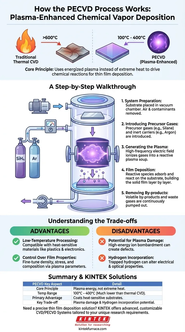
At its core, Plasma-Enhanced Chemical Vapor Deposition (PECVD) is a process for creating a thin solid film on a surface, known as a substrate, by using an energized gas called a plasma. Unlike traditional methods that rely on high heat, PECVD uses the energy from the plasma to drive the chemical reactions needed to transform precursor gases into a solid film. This fundamental difference allows for deposition at significantly lower temperatures.
The central advantage of PECVD is its use of plasma to energize reactant gases, which enables high-quality film deposition at temperatures low enough to be safe for sensitive substrates like plastics and integrated circuits. This unlocks capabilities impossible with high-temperature thermal processes.
The Principle: Energy Transfer Without Extreme Heat
The Goal: From Gas to Solid Film
All Chemical Vapor Deposition (CVD) methods share a common goal: to take precursor chemicals in a gas state and make them react to form a solid, uniform coating on a substrate.
The process is like a microscopic construction project, where individual molecules are the building blocks for a new surface layer.
The Problem with Traditional Methods
Traditional thermal CVD works by heating the substrate to very high temperatures (often >600°C). This intense heat provides the energy needed to break down the precursor gases and initiate the chemical reactions for film growth.
However, such high temperatures can easily damage or destroy many substrates, including polymers, plastics, and complex electronic components.
The PECVD Solution: Energized Plasma
PECVD solves this problem by creating energy in a different way. Instead of relying only on heat, it introduces energy by applying a powerful electric field to the precursor gases inside a vacuum chamber.
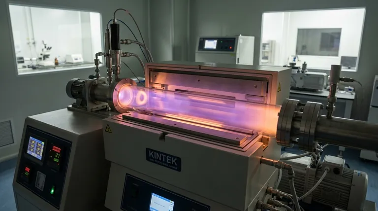
This electric field strips electrons from the gas molecules, creating a highly reactive, ionized gas known as a plasma. This plasma contains ions, electrons, and neutral radicals that are full of the energy needed to drive the deposition reactions, all without requiring extreme heat.
A Step-by-Step Walkthrough of the Process
Step 1: System Preparation
The process begins with placing the substrate inside a vacuum chamber. The chamber is then pumped down to a very low pressure, removing air and other contaminants that could interfere with the reaction.
Step 2: Introducing Precursor Gases
Once under vacuum, one or more precursor gases (such as silane, SiH4, for silicon nitride films) are introduced into the chamber at a controlled rate. These are the source materials for the film.
Often, an inert carrier gas like argon or nitrogen is mixed in to help stabilize the process.
Step 3: Generating the Plasma
A high-frequency electric field is applied between two electrodes within the chamber. This powerful field energizes the gas mixture, igniting it into a glowing plasma.
This plasma is a soup of highly reactive chemical species that are now primed for deposition.
Step 4: Film Deposition on the Substrate
The reactive ions and radicals from the plasma diffuse and adsorb onto the relatively cool surface of the substrate. There, they undergo a series of chemical reactions, bonding to the surface and to each other.
This process builds up the desired material layer by layer, forming a solid, thin film with a thickness that can be controlled from a few nanometers to several micrometers.
Step 5: Removing By-products
The chemical reactions that form the film also create volatile by-products. These waste gases are continuously removed from the chamber by the vacuum pump, ensuring a clean and controlled deposition process.
Understanding the Trade-offs
Advantage: Low-Temperature Processing
This is the primary reason for choosing PECVD. The ability to deposit films at temperatures typically between 100°C and 400°C makes it compatible with a vast range of heat-sensitive materials that thermal CVD would destroy.
Advantage: Control Over Film Properties
By adjusting parameters like gas flow, pressure, and the power of the electric field, an operator can fine-tune the plasma's energy and density. This provides direct control over the final film's properties, such as its density, stress, and chemical composition.
Disadvantage: Potential for Plasma Damage
The high-energy ions that make the process so effective can also be a drawback. In some cases, these ions can bombard the substrate or the growing film with enough force to create defects or damage, impacting performance.
Disadvantage: Hydrogen Incorporation
Many common precursors (like silane, SiH4, and ammonia, NH3) contain hydrogen. In a PECVD process, this hydrogen can become trapped within the deposited film, which can alter its electrical and optical properties. This is a well-known trade-off that often requires post-processing steps to mitigate.
Making the Right Choice for Your Application
Choosing the correct deposition method requires understanding your material constraints and final goal.
- If your primary focus is coating temperature-sensitive substrates like plastics or electronics: PECVD is almost always the correct choice due to its low-temperature operation.
- If your primary focus is achieving the highest film purity on a robust substrate: Thermal CVD may be a better option, as it avoids plasma-induced damage and hydrogen incorporation.
- If your primary focus is fine-tuning specific film properties like mechanical stress: PECVD offers a wider control window by allowing you to manipulate plasma parameters directly.
Ultimately, selecting the right technique depends on balancing the need for low-temperature processing against the desired purity and structure of the final film.
Summary Table:
| Key Aspect | PECVD Process Detail |
|---|---|
| Core Principle | Uses plasma energy instead of extreme heat to drive chemical reactions for deposition. |
| Typical Temperature Range | 100°C to 400°C, much lower than thermal CVD (>600°C). |
| Primary Advantage | Enables coating of heat-sensitive materials (e.g., plastics, integrated circuits). |
| Key Trade-off | Potential for plasma-induced substrate damage and hydrogen incorporation in films. |
Need a precise thin film deposition solution for your sensitive materials?
Leveraging exceptional R&D and in-house manufacturing, KINTEK provides diverse laboratories with advanced high-temperature furnace solutions, including our specialized CVD/PECVD Systems. Our strong deep customization capability allows us to tailor PECVD systems to precisely meet your unique experimental requirements, ensuring optimal film quality and process efficiency.
Contact us today to discuss how our PECVD expertise can enhance your research and development!
Visual Guide
Related Products
- RF PECVD System Radio Frequency Plasma Enhanced Chemical Vapor Deposition
- Slide PECVD Tube Furnace with Liquid Gasifier PECVD Machine
- Inclined Rotary Plasma Enhanced Chemical Deposition PECVD Tube Furnace Machine
- Inclined Rotary Plasma Enhanced Chemical Deposition PECVD Tube Furnace Machine
- Cylindrical Resonator MPCVD Machine System for Lab Diamond Growth
People Also Ask
- What are the advantages of PECVD in film deposition? Achieve Low-Temp, High-Quality Coatings
- What is PECVD specification? A Guide to Choosing the Right System for Your Lab
- How are deposition rates and film properties controlled in PECVD? Master Key Parameters for Optimal Thin Films
- How is silicon dioxide deposited from tetraethylorthosilicate (TEOS) in PECVD? Achieve Low-Temperature, High-Quality SiO2 Films
- What is RF in PECVD? A Critical Control for Plasma Deposition


