At its core, Plasma-Enhanced Chemical Vapor Deposition (PECVD) is a manufacturing process used to deposit extremely thin, high-quality films of material onto a substrate. Unlike traditional methods that rely on extreme heat, PECVD uses an energized gas, or plasma, to drive the chemical reactions, allowing the process to occur at much lower temperatures.
The central challenge in thin-film deposition is that high heat can damage sensitive electronic components or substrates. PECVD solves this by replacing raw thermal energy with the targeted energy of a plasma, enabling the creation of advanced materials on a wider range of products without causing thermal damage.
How PECVD Works: From Gas to Solid Film
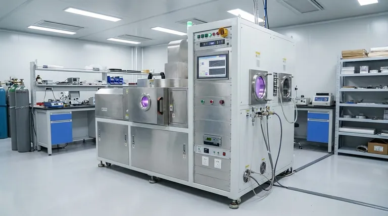
The PECVD process is a carefully controlled sequence that takes place inside a sealed vacuum chamber. It transforms specific gases into a solid, uniform layer on a target surface.
The Vacuum Chamber Environment
First, a substrate is placed inside a vacuum chamber. The pressure is lowered significantly, typically to less than 0.1 Torr, creating a controlled environment free of contaminants.
Precursor gases, such as silane (SiH₄) for silicon films or ammonia (NH₃) for nitride films, are then introduced into the chamber.
Creating the Plasma
An electric field is applied across electrodes within the chamber. This field energizes free electrons, causing them to collide with the neutral precursor gas molecules.
These high-energy collisions strip electrons from the gas molecules, creating a mix of ions, electrons, and neutral species known as a plasma. This plasma is the key to the entire process.
The Deposition Process
The highly reactive ions and radicals within the plasma are then drawn to the substrate's surface.
Once there, they bond to the surface and to each other, gradually building up a thin, solid, and highly uniform film. The temperature, pressure, and gas composition are all precisely controlled to manage the final film's properties.
The Core Advantages of Using Plasma
The use of plasma instead of high heat is not just a minor difference; it fundamentally changes what is possible in materials engineering and manufacturing.
The Low-Temperature Advantage
This is the most critical benefit of PECVD. Traditional Chemical Vapor Deposition (CVD) often requires temperatures exceeding 600°C, which would destroy complex electronics, flexible plastics, or other sensitive substrates.
PECVD operates at much lower temperatures, often below 350°C, making it ideal for depositing films on fully fabricated microchips, solar cells, and LEDs without damaging them.
Superior Speed and Efficiency
Plasma-driven reactions are extremely energetic and efficient. This results in deposition rates that can be orders of magnitude faster than conventional CVD.
For example, depositing a silicon nitride film can be over 100 times faster with PECVD, dramatically increasing manufacturing throughput.
High-Quality Film Formation
The resulting films are known for their excellent quality. They exhibit strong adhesion to the substrate and have a highly uniform thickness.
Furthermore, PECVD films typically have fewer defects like pinholes and a reduced tendency to crack, leading to more reliable and durable components.
Versatility and Control
By precisely adjusting the plasma parameters, gas mixtures, and pressure, engineers can tune the properties of the deposited film.
This allows for the creation of films with different densities, chemical compositions, and electrical characteristics, all from the same system.
Understanding the Trade-offs and Considerations
While powerful, PECVD is not a universal solution. Understanding its limitations is key to using it effectively.
Potential for Plasma-Induced Damage
The same high-energy ions that enable low-temperature deposition can sometimes cause physical damage to extremely sensitive substrate surfaces through ion bombardment. This requires careful tuning of the plasma energy for delicate applications.
Process and Equipment Complexity
A PECVD system, with its vacuum pumps, gas handling, and radio-frequency (RF) power source for the plasma, is more complex and expensive than a simple thermal CVD furnace. The process itself also has more variables to control.
Film Composition and Purity
Because precursor gases (like silane, SiH₄) often contain hydrogen, some of this hydrogen can be incorporated into the final film. While sometimes desirable, this can be an unintentional impurity that affects the film's electrical or optical properties.
Key Applications Across Industries
PECVD's unique combination of low temperature, speed, and quality has made it an indispensable technique in several high-tech fields.
In Semiconductor Manufacturing
PECVD is a workhorse in fabricating microchips. It is used to deposit dielectric layers that insulate conductive pathways, passivation layers that protect the chip from the environment, and films for creating capacitors and transistors.
For Solar Cells and LEDs
The efficiency of modern solar cells and the brightness of LEDs depend on high-quality thin films. PECVD is essential for creating the anti-reflective coatings and passivation layers in solar cells and for fabricating the structures inside high-brightness LEDs.
In Advanced Materials and Devices
The applications extend to fabricating Micro-Electro-Mechanical Systems (MEMS), creating protective, corrosion-resistant coatings on medical devices, and even depositing advanced materials like vertically aligned graphene.
Making the Right Choice for Your Goal
Selecting a deposition method depends entirely on the requirements of your substrate and desired film properties.
- If your primary focus is depositing on temperature-sensitive substrates like plastics or completed electronics: PECVD is the definitive choice over high-temperature methods.
- If your primary focus is high throughput and manufacturing speed: PECVD's rapid deposition rates offer a significant advantage for production environments.
- If your primary focus is achieving the highest possible film purity and crystallinity: You may need to evaluate if a higher-temperature process like conventional CVD is necessary, despite its limitations.
By replacing intense heat with controlled plasma energy, PECVD provides the precision and flexibility required for building the next generation of advanced materials and devices.
Summary Table:
| Feature | PECVD | Traditional CVD |
|---|---|---|
| Process Temperature | Low (Often < 350°C) | High (Often > 600°C) |
| Primary Energy Source | Plasma | Thermal (Heat) |
| Key Advantage | Ideal for sensitive substrates | High film purity & crystallinity |
| Deposition Speed | Fast | Slower |
| Typical Applications | Semiconductors, Solar Cells, LEDs | High-temperature substrates |
Ready to integrate PECVD technology into your lab?
Leveraging exceptional R&D and in-house manufacturing, KINTEK provides diverse laboratories with advanced high-temperature furnace solutions. Our product line, including PECVD Systems, is complemented by our strong deep customization capability to precisely meet your unique experimental requirements for thin-film deposition.
Contact our experts today to discuss how a KINTEK PECVD system can accelerate your research and development.
Visual Guide

Related Products
- Slide PECVD Tube Furnace with Liquid Gasifier PECVD Machine
- RF PECVD System Radio Frequency Plasma Enhanced Chemical Vapor Deposition
- Inclined Rotary Plasma Enhanced Chemical Deposition PECVD Tube Furnace Machine
- Inclined Rotary Plasma Enhanced Chemical Deposition PECVD Tube Furnace Machine
- Multi Heating Zones CVD Tube Furnace Machine for Chemical Vapor Deposition Equipment
People Also Ask
- What plasma source is used in PE-CVD tube furnaces? Unlock Low-Temperature, High-Quality Deposition
- What is plasma in the context of PECVD? Unlock Low-Temperature Thin Film Deposition
- In which industries is the tube furnace commonly used? Essential for Materials Science, Energy, and More
- How does a hydrogen reduction environment in an industrial tube furnace facilitate gold-copper alloy microspheres?
- What are the disadvantages of tube furnace cracking when processing heavy raw materials? Avoid Costly Downtime and Inefficiency


