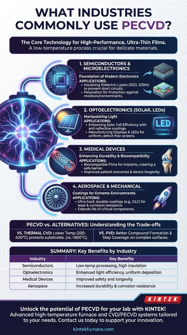
At its core, Plasma-Enhanced Chemical Vapor Deposition (PECVD) is a foundational technology used across any industry that requires high-performance, ultra-thin films deposited onto a surface. It is most prominently used in semiconductors and microelectronics, optoelectronics (including solar cells and LEDs), medical devices, and aerospace for creating protective, insulating, or optically active layers.
The true value of PECVD is its ability to deposit high-quality films at much lower temperatures than traditional methods. This single advantage unlocks its use on delicate, temperature-sensitive materials, making it indispensable for manufacturing modern high-tech components.
The Foundation of Modern Electronics
PECVD is not just an option in the semiconductor industry; it is a cornerstone of modern fabrication. Its low-temperature process is critical for building the complex, layered structures of integrated circuits without damaging the underlying components.
Insulating Dielectric Layers
The primary use of PECVD in microelectronics is to deposit thin films of silicon dioxide (SiO2) and silicon nitride (Si3N4). These materials act as superb electrical insulators.
They are used to isolate conductive pathways from one another on a chip, preventing short circuits and ensuring the device functions correctly. Without this precise insulation, modern microprocessors would be impossible to build.
Passivation for Protection
Chips are incredibly sensitive to moisture and contaminants. PECVD is used to apply a final passivation layer (typically silicon nitride) over the entire device.
This durable, chemically inert film seals the chip, protecting it from environmental damage and dramatically increasing its reliability and lifespan. This is critical for electronics in all fields, from consumer devices to automotive and military systems.
Manipulating Light in Optoelectronics
The ability to control a material's optical properties is vital for devices that generate or interact with light. PECVD provides the precision needed to create films that manage light with exceptional efficiency.
Enhancing Solar Cell Efficiency
In the photovoltaics (solar cell) industry, efficiency is everything. PECVD is used to apply an anti-reflective coating, often of silicon nitride, to the surface of the solar cell.
This layer is engineered to minimize the amount of sunlight that reflects off the surface, allowing more light to enter the cell and be converted into electricity. It also serves as a passivation layer, further improving performance.
Manufacturing Displays and LEDs
For flat-panel displays and LEDs, PECVD is used to deposit the various thin films that form the structure of pixels and light-emitting components. Its uniformity over large areas is essential for producing high-quality, defect-free screens.
Enhancing Durability and Biocompatibility
Beyond electronics, PECVD is a surface modification tool used to give ordinary materials extraordinary properties. This is crucial in demanding mechanical and medical environments.
Coatings for Extreme Environments
In the aerospace and mechanical engineering sectors, components are exposed to extreme temperatures, corrosion, and wear. PECVD is used to deposit ultra-hard, durable coatings like diamond-like carbon (DLC).
These films dramatically increase the hardness and corrosion resistance of a surface, extending the life of tools, engine parts, and other critical components.
Biocompatible Films for Medical Devices
When a device is implanted in the human body, it must not cause an adverse reaction. PECVD is used to coat medical implants, such as stents or joint replacements, with biocompatible films.
These inert coatings create a safe barrier between the implant material and the body's tissues, improving patient outcomes and device longevity.
Understanding the Trade-offs: PECVD vs. Alternatives
While powerful, PECVD is one of several deposition technologies. Understanding its place is key to appreciating its value.
PECVD vs. Thermal CVD
Traditional Chemical Vapor Deposition (CVD) uses high temperatures (often >600°C) to drive chemical reactions. This produces very pure, high-quality films but can damage or melt many substrates, including a finished silicon wafer or plastic.
PECVD uses plasma to energize the reactive gases, allowing deposition to occur at much lower temperatures (typically 200-400°C). This is its single greatest advantage, though the resulting films may have slightly lower purity than a high-temperature CVD film.
PECVD vs. PVD
Physical Vapor Deposition (PVD) is another low-temperature process that involves physically sputtering a target material onto a substrate. PVD is generally simpler and better for depositing pure metals.
However, PECVD excels at forming compounds like oxides and nitrides, and it offers better coverage over complex, non-flat surfaces (known as "step coverage").
Making the Right Choice for Your Goal
Your choice of technology depends entirely on the problem you need to solve.
- If your primary focus is fabricating complex microelectronics: PECVD is the industry standard for depositing high-quality dielectric and passivation layers without damaging sensitive components.
- If your primary focus is improving optical efficiency: PECVD is essential for creating the anti-reflective and passivation coatings needed for high-performance solar cells, LEDs, and displays.
- If your primary focus is creating durable or biocompatible surfaces: PECVD provides the means to apply highly functional coatings that protect against wear, corrosion, or biological rejection.
Ultimately, PECVD is the go-to solution for creating high-performance compound films when the integrity of the underlying material must be preserved.
Summary Table:
| Industry | Common Applications | Key Benefits |
|---|---|---|
| Semiconductors | Dielectric layers, passivation | Low-temperature processing, high insulation |
| Optoelectronics | Anti-reflective coatings, LEDs | Enhanced light efficiency, uniform deposition |
| Medical Devices | Biocompatible coatings | Improved safety and longevity |
| Aerospace | Protective coatings (e.g., DLC) | Increased durability and corrosion resistance |
Unlock the potential of PECVD for your lab with KINTEK! Leveraging exceptional R&D and in-house manufacturing, we provide advanced high-temperature furnace solutions tailored to your needs. Our product line includes Muffle, Tube, Rotary Furnaces, Vacuum & Atmosphere Furnaces, and CVD/PECVD Systems, all backed by strong deep customization capabilities to meet unique experimental requirements. Whether you're in semiconductors, optoelectronics, medical devices, or aerospace, KINTEK delivers precise, reliable equipment to enhance your processes. Contact us today to discuss how we can support your innovation and efficiency goals!
Visual Guide
Related Products
- Slide PECVD Tube Furnace with Liquid Gasifier PECVD Machine
- RF PECVD System Radio Frequency Plasma Enhanced Chemical Vapor Deposition
- Inclined Rotary Plasma Enhanced Chemical Deposition PECVD Tube Furnace Machine
- Inclined Rotary Plasma Enhanced Chemical Deposition PECVD Tube Furnace Machine
- Multi Heating Zones CVD Tube Furnace Machine for Chemical Vapor Deposition Equipment
People Also Ask
- What are the typical conditions for plasma-enhanced CVD processes? Achieve Low-Temperature Thin Film Deposition
- How does a hydrogen reduction environment in an industrial tube furnace facilitate gold-copper alloy microspheres?
- What are the disadvantages of tube furnace cracking when processing heavy raw materials? Avoid Costly Downtime and Inefficiency
- What are the advantages of using a tube furnace CVD system for Cu(111)/graphene? Superior Scalability and Quality
- In which industries is the tube furnace commonly used? Essential for Materials Science, Energy, and More


