At its core, Plasma-Enhanced Chemical Vapor Deposition (PECVD) is a method for depositing thin films onto a substrate. It differs from standard Chemical Vapor Deposition (CVD) by using plasma to energize the precursor gases, which allows the deposition process to occur at significantly lower temperatures. While traditional CVD relies purely on high heat to drive chemical reactions, PECVD uses an electric field to create a reactive plasma environment.
The fundamental choice between CVD and PECVD is a choice of energy source. CVD uses thermal energy (high heat), while PECVD uses plasma energy. This single difference dictates which materials you can coat, the properties of the resulting film, and the overall cost and complexity of the process.

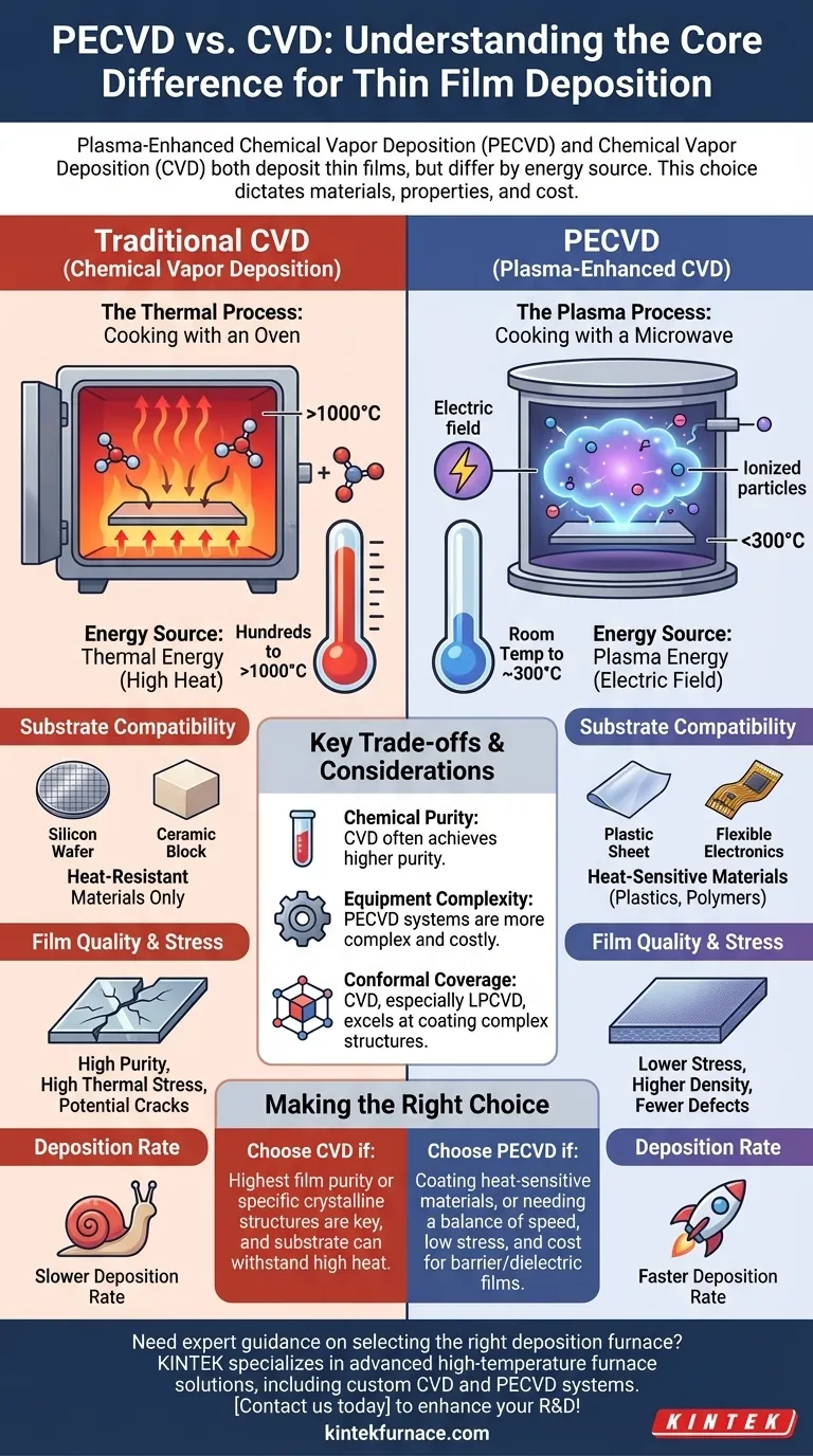
The Core Difference: How Energy is Supplied
To understand the distinction, think of it as the difference between cooking with a conventional oven versus a microwave. Both cook the food, but they use entirely different energy transfer mechanisms.
How Traditional CVD Works
Traditional CVD is a purely thermal process. Precursor gases are introduced into a high-temperature furnace, often operating from several hundred to over a thousand degrees Celsius.
The intense heat provides the necessary activation energy to break down the gas molecules and cause them to react and deposit as a solid film on the heated substrate. It's simple, robust, and effective.
How PECVD Works
PECVD introduces a new ingredient: plasma. Instead of relying solely on heat, an electric field (typically radio frequency or microwave) is applied to the gas, ionizing it and creating a plasma.
This plasma is a highly reactive soup of ions, electrons, and free radicals. These energized particles have enough energy to drive the chemical reactions for deposition, even at much lower substrate temperatures (from room temperature to around 300°C).
Practical Implications of the Temperature Difference
The lower operating temperature of PECVD is not just a minor detail; it is the defining advantage that opens up entirely new applications and capabilities.
Substrate Compatibility
This is the most significant consequence. The high heat of CVD limits its use to substrates that can withstand extreme temperatures, such as silicon wafers, ceramics, and certain metals.
PECVD’s low-temperature process allows for the deposition of high-quality films on heat-sensitive materials like plastics, polymers, and complex electronic devices that would be damaged or destroyed by a traditional CVD process.
Film Quality and Stress
High temperatures can introduce significant thermal stress into a film as it cools, potentially causing cracks or delamination. This is especially true when the film and substrate have different thermal expansion coefficients.
Because PECVD operates at lower temperatures, the resulting films typically exhibit much lower internal stress, superior density, and fewer pinhole defects.
Deposition Rate and Efficiency
The energized plasma in PECVD often leads to higher deposition rates compared to thermal CVD. This can reduce manufacturing time and energy consumption, making the process more cost-effective for many applications.
Understanding the Trade-offs
Choosing PECVD is not without its compromises. The introduction of plasma adds complexity and creates a different set of challenges.
Chemical Purity and Contamination
The plasma environment is chemically complex. This can lead to the incorporation of other elements, particularly hydrogen from precursor gases, into the deposited film.
While not always a negative, this means that films produced by traditional thermal CVD can often achieve a higher level of chemical purity, which is critical for certain high-performance electronic applications.
Equipment Complexity
A PECVD system is inherently more complex than a standard CVD furnace. It requires a vacuum chamber, a gas delivery system, and a power source (like an RF generator) to create and sustain the plasma. This can increase the initial capital cost and maintenance requirements.
Conformal Coverage
Traditional CVD, especially Low-Pressure CVD (LPCVD), is known for its excellent ability to coat complex, three-dimensional structures uniformly (known as conformality).
While PECVD can achieve good coverage, the line-of-sight and plasma-sheath effects can sometimes make it more challenging to achieve perfectly conformal coatings on intricate topographies compared to some thermal CVD techniques.
Making the Right Choice for Your Goal
The decision to use PECVD or CVD is not about which is "better" but which is the correct tool for your specific engineering objective.
- If your primary focus is coating heat-sensitive materials (like polymers or flexible electronics): PECVD is the definitive and often only choice due to its low-temperature operation.
- If your primary focus is achieving the highest possible film purity or specific crystalline structures: Traditional high-temperature CVD is often the superior method, provided your substrate can tolerate the heat.
- If your primary focus is balancing deposition speed, low stress, and cost for general-purpose barrier or dielectric films: PECVD provides a powerful and highly versatile solution.
Ultimately, understanding the fundamental difference between thermal energy and plasma energy empowers you to select the precise deposition technique for your material and application.
Summary Table:
| Feature | CVD | PECVD |
|---|---|---|
| Energy Source | Thermal (high heat) | Plasma (electric field) |
| Operating Temperature | High (hundreds to over 1000°C) | Low (room temp to ~300°C) |
| Substrate Compatibility | Heat-resistant materials (e.g., silicon, ceramics) | Heat-sensitive materials (e.g., plastics, polymers) |
| Film Quality | High purity, potential for thermal stress | Lower stress, higher density, fewer defects |
| Deposition Rate | Slower | Faster |
| Equipment Complexity | Lower | Higher |
Need expert guidance on selecting the right deposition furnace for your lab? KINTEK specializes in advanced high-temperature furnace solutions, including CVD and PECVD systems, tailored to your unique experimental needs. Leveraging our exceptional R&D and in-house manufacturing, we offer deep customization to ensure optimal performance for your materials and applications. Contact us today to discuss how our products can enhance your research and development!
Visual Guide
Related Products
- RF PECVD System Radio Frequency Plasma Enhanced Chemical Vapor Deposition
- Slide PECVD Tube Furnace with Liquid Gasifier PECVD Machine
- Inclined Rotary Plasma Enhanced Chemical Deposition PECVD Tube Furnace Machine
- Inclined Rotary Plasma Enhanced Chemical Deposition PECVD Tube Furnace Machine
- Cylindrical Resonator MPCVD Machine System for Lab Diamond Growth
People Also Ask
- What are some promising applications of PECVD-prepared 2D materials? Unlock Advanced Sensing and Optoelectronics
- How are deposition rates and film properties controlled in PECVD? Master Key Parameters for Optimal Thin Films
- What is PECVD specification? A Guide to Choosing the Right System for Your Lab
- What are the advantages of PECVD in film deposition? Achieve Low-Temp, High-Quality Coatings
- What are the applications of plasma enhanced chemical vapor deposition? Key Uses in Electronics, Optics & Materials


