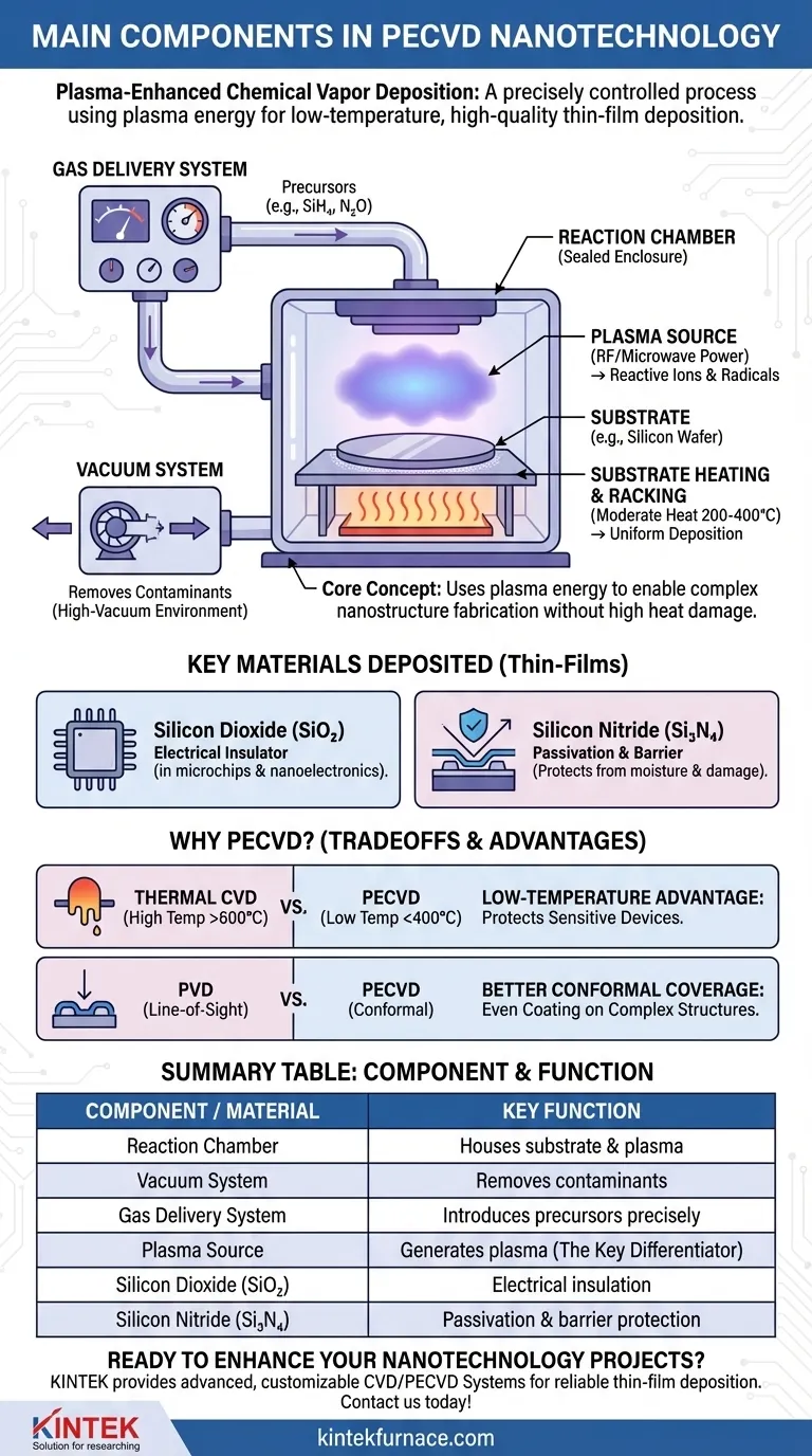
At its core, Plasma-Enhanced Chemical Vapor Deposition (PECVD) involves two sets of "components": the physical hardware of the system and the thin-film materials it is designed to create. The key hardware includes a reaction chamber, vacuum pumps, a gas delivery system, and a plasma-generating power source. The most common materials, or "components," deposited in nanotechnology are high-purity films of silicon dioxide and silicon nitride.
The central concept to grasp is that PECVD is not merely a collection of parts, but a precisely controlled process. It uses the energy from plasma, rather than high heat, to deposit critical thin-film materials, enabling the fabrication of complex and delicate nanostructures that would be destroyed by traditional high-temperature methods.
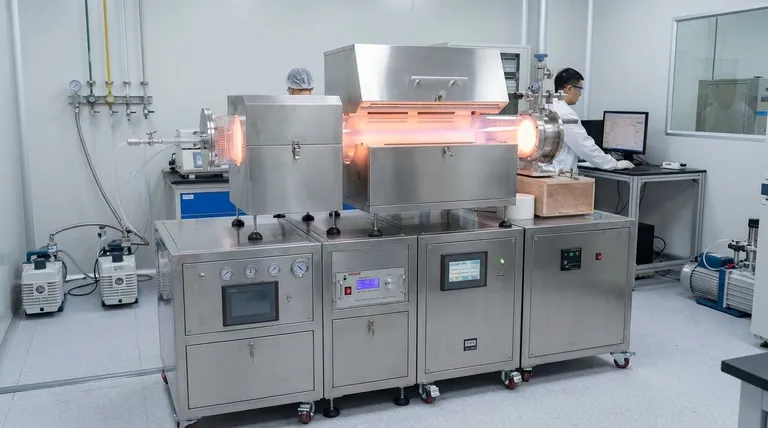
The Anatomy of a PECVD System
To understand how PECVD works, it is essential to understand the function of its core physical components. Each part plays a critical role in controlling the environment to produce a uniform, high-quality thin film.
The Reaction Chamber
This is the heart of the system where the deposition takes place. It is a sealed enclosure that houses the substrate (e.g., a silicon wafer) and is designed to withstand a vacuum and contain the plasma.
The Vacuum System
A system of pumps creates a high-vacuum environment inside the chamber. This is crucial for removing contaminants like air and water vapor, which would otherwise interfere with the chemical reactions and compromise the purity of the deposited film.
The Gas Delivery System
This network precisely introduces specific precursor gases into the reaction chamber. Using components like mass flow controllers, it ensures the exact mixture and flow rate of gases needed to form the desired material. For example, silane (SiH₄) and nitrous oxide (N₂O) might be used to create silicon dioxide.
The Plasma Source (The Key Differentiator)
This is what puts the "PE" in PECVD. A radio frequency (RF) or microwave power source is used to ignite the precursor gases, turning them into a plasma. This plasma is an energized state of matter containing reactive ions and radicals that can form the desired film at much lower temperatures (typically 200-400°C) than conventional CVD (often >600°C).
Substrate Heating and Racking
While PECVD is a low-temperature process, the substrate is often moderately heated to enhance film properties and surface mobility. Racking holds the substrates in a precise orientation within the chamber to ensure uniform deposition across their surface.
Key Materials Deposited by PECVD
In nanotechnology and semiconductor manufacturing, PECVD is most valued for its ability to deposit high-quality dielectric and passivation layers.
Silicon Dioxide (SiO₂)
This material is an excellent electrical insulator. In PECVD, it is deposited as a thin film to isolate conductive layers from one another in microchips and other nanoelectronic devices. It is a fundamental building block for creating transistors and capacitors.
Silicon Nitride (Si₃N₄)
Silicon nitride is a hard, dense material that serves as an exceptional barrier. It is commonly used as a passivation layer to protect the finished device from moisture, mobile ions, and physical scratches. It can also serve as a chemical-resistant mask during etching steps.
Understanding the Trade-offs: PECVD vs. Alternatives
No single fabrication technique is perfect for every application. Choosing PECVD requires understanding its advantages and limitations compared to other deposition methods like traditional thermal CVD or Physical Vapor Deposition (PVD).
The Low-Temperature Advantage
This is the primary reason for choosing PECVD. It allows for deposition on top of fully-formed devices with sensitive materials (like aluminum wiring) that would be damaged or melted by the high heat of thermal CVD.
Film Quality and Impurities
The films from PECVD are high quality, but because the process uses hydrogen-containing precursors (like silane), the resulting films often contain residual hydrogen. For applications demanding the absolute highest purity and density, high-temperature thermal CVD may still be superior, assuming the substrate can tolerate the heat.
Conformal Coverage
Compared to PVD (like sputtering), which is a line-of-sight process, PECVD offers better "conformal coverage." This means it can more evenly coat the complex, three-dimensional topographies found in advanced nanostructures, ensuring there are no gaps or weak points in the deposited layer.
Making the Right Choice for Your Goal
Your choice of deposition technology depends entirely on the requirements of your final device.
- If your primary focus is creating robust insulating layers on sensitive electronics: PECVD is the industry standard for depositing high-quality silicon dioxide at temperatures that will not damage underlying components.
- If your primary focus is protecting or encapsulating a finished device: PECVD is ideal for depositing dense silicon nitride passivation layers that guard against moisture and contamination.
- If your primary focus is achieving the highest possible film purity and density: You may need to consider traditional high-temperature CVD, but only if your substrate and existing device structures can withstand the extreme thermal budget.
By understanding both the machinery and the materials, you can effectively leverage PECVD to achieve precise and reliable outcomes in your nanofabrication work.
Summary Table:
| Component/Material | Key Function | Common Examples |
|---|---|---|
| Reaction Chamber | Houses substrate and plasma for deposition | Sealed enclosure |
| Vacuum System | Removes contaminants for high-purity films | Vacuum pumps |
| Gas Delivery System | Introduces precursor gases precisely | Mass flow controllers |
| Plasma Source | Generates plasma for low-temperature deposition | RF or microwave power |
| Silicon Dioxide (SiO₂) | Electrical insulation in microchips | Dielectric layers |
| Silicon Nitride (Si₃N₄) | Passivation and barrier protection | Moisture-resistant films |
Ready to enhance your nanotechnology projects with advanced PECVD solutions? KINTEK leverages exceptional R&D and in-house manufacturing to provide diverse laboratories with high-temperature furnace solutions, including CVD/PECVD Systems. Our strong deep customization capability ensures we precisely meet your unique experimental requirements for reliable, high-quality thin-film deposition. Contact us today to discuss how we can support your innovations!
Visual Guide
Related Products
- RF PECVD System Radio Frequency Plasma Enhanced Chemical Vapor Deposition
- Slide PECVD Tube Furnace with Liquid Gasifier PECVD Machine
- Inclined Rotary Plasma Enhanced Chemical Deposition PECVD Tube Furnace Machine
- Inclined Rotary Plasma Enhanced Chemical Deposition PECVD Tube Furnace Machine
- Cylindrical Resonator MPCVD Machine System for Lab Diamond Growth
People Also Ask
- What is RF in PECVD? A Critical Control for Plasma Deposition
- What are the advantages of PECVD in film deposition? Achieve Low-Temp, High-Quality Coatings
- What is PECVD specification? A Guide to Choosing the Right System for Your Lab
- What are the applications of plasma enhanced chemical vapor deposition? Key Uses in Electronics, Optics & Materials
- How is silicon dioxide deposited from tetraethylorthosilicate (TEOS) in PECVD? Achieve Low-Temperature, High-Quality SiO2 Films


