In modern microelectronics, Plasma-Enhanced Chemical Vapor Deposition (PECVD) is a critical fabrication step because it deposits essential, high-quality thin films at low temperatures. This capability is fundamental for building today's complex, multi-layered circuits without damaging previously fabricated structures or compromising the device's electrical integrity.
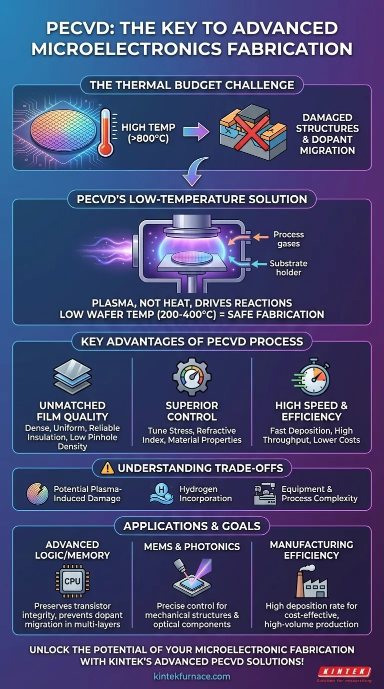
The core challenge in fabricating advanced microchips is not merely depositing materials, but doing so within an increasingly restrictive "thermal budget." PECVD solves this by using the energy of a plasma, rather than high heat, to drive chemical reactions, enabling the creation of devices that would be impossible with conventional high-temperature methods.
The Core Challenge: A Shrinking Thermal Budget
At the heart of PECVD's importance is the concept of a thermal budget—the total amount of heat a semiconductor wafer can be exposed to during its entire manufacturing process before performance is degraded.
Why High Temperatures Are a Problem
As devices shrink, they become incredibly sensitive to heat. High temperatures, like those used in traditional Chemical Vapor Deposition (CVD), cause two primary problems.
First, they can damage delicate structures and materials already present on the wafer. Second, and more critically, they cause dopants—impurities intentionally added to silicon to control its electrical properties—to migrate or diffuse from their intended locations. This migration ruins the precise electrical engineering of the transistors, rendering the device useless.
PECVD’s Solution: Plasma, Not Heat
PECVD circumvents this limitation by creating a plasma, an ionized gas, within the reaction chamber. This plasma provides the necessary energy to break down precursor gases and drive the chemical reactions needed for film deposition.
Because the energy comes from the plasma rather than thermal agitation, the wafer itself can be kept at a much lower temperature (typically 200-400°C), well below the threshold that causes damage or dopant migration.
Key Advantages of the PECVD Process
Beyond solving the temperature problem, PECVD provides a unique combination of control, quality, and speed that is essential for high-volume manufacturing.
Unmatched Film Quality and Integrity
PECVD creates films that are dense, uniform, and adhere well to the substrate. This process results in fewer pinholes and a lower likelihood of cracking, which is critical for creating reliable insulation and protective layers. The resulting films offer excellent resistance to corrosion and humidity.
Superior Control Over Material Properties
By adjusting gas composition, pressure, and plasma power, engineers can precisely tune the properties of the deposited film. This includes mechanical stress, refractive index (vital for optical components), and hardness. This level of control is essential for performance-critical applications.
High Deposition Speed and Efficiency
The plasma-driven reactions in PECVD are extremely fast. For certain materials like silicon nitride, deposition can be over 100 times faster than in a conventional furnace process. This dramatic increase in throughput directly lowers manufacturing costs and increases factory output.
Understanding the Trade-offs
While indispensable, PECVD is not without its complexities. Acknowledging its limitations is key to its successful implementation.
Potential for Plasma-Induced Damage
The high-energy ions within the plasma can, if not properly controlled, physically damage the surface of the wafer. Process engineers must carefully optimize plasma conditions to maximize deposition benefits while minimizing this potential side effect.
Hydrogen Incorporation
Many PECVD precursor gases (like silane, SiH₄) contain hydrogen. This hydrogen can become incorporated into the deposited film, which may affect its electrical properties over the device's lifetime. Post-deposition annealing is often required to manage this.
Equipment and Process Complexity
PECVD systems are more complex and expensive than simple thermal furnaces. They require sophisticated radio-frequency (RF) power supplies, vacuum systems, and process controls to maintain stability and repeatability.
Making the Right Choice for Your Goal
PECVD is not just one tool; it is a versatile platform whose benefits can be leveraged for different outcomes. Understanding your primary goal is key to appreciating its role.
- If your primary focus is fabricating advanced logic or memory: PECVD's low-temperature processing is non-negotiable for preserving the integrity of transistors and preventing dopant migration in multi-layer interconnects.
- If your primary focus is MEMS or photonic devices: PECVD's ability to precisely control film stress and refractive index is your most critical advantage for building functional mechanical structures and light guides.
- If your primary focus is manufacturing efficiency: PECVD's high deposition rate offers a significant throughput advantage, enabling cost-effective, high-volume production of insulating and passivation layers.
Ultimately, PECVD is an enabling technology that allows fabrication processes to meet the relentless demands of device miniaturization and functional complexity.
Summary Table:
| Key Aspect | Importance in Microelectronics |
|---|---|
| Low-Temperature Deposition | Prevents damage and dopant migration, crucial for multi-layer devices |
| Film Quality | Ensures dense, uniform, and reliable insulation and passivation layers |
| Material Control | Allows precise tuning of stress, refractive index, and other properties |
| Deposition Speed | Increases throughput, reducing manufacturing costs and time |
| Thermal Budget Management | Essential for advanced logic, memory, MEMS, and photonic devices |
Unlock the full potential of your microelectronic fabrication with KINTEK's advanced PECVD solutions! Leveraging exceptional R&D and in-house manufacturing, we provide diverse laboratories with high-temperature furnace systems like CVD/PECVD, tailored to your unique needs. Our expertise ensures precise control, efficiency, and reliability for your projects. Contact us today to discuss how our customized solutions can enhance your device performance and accelerate innovation!
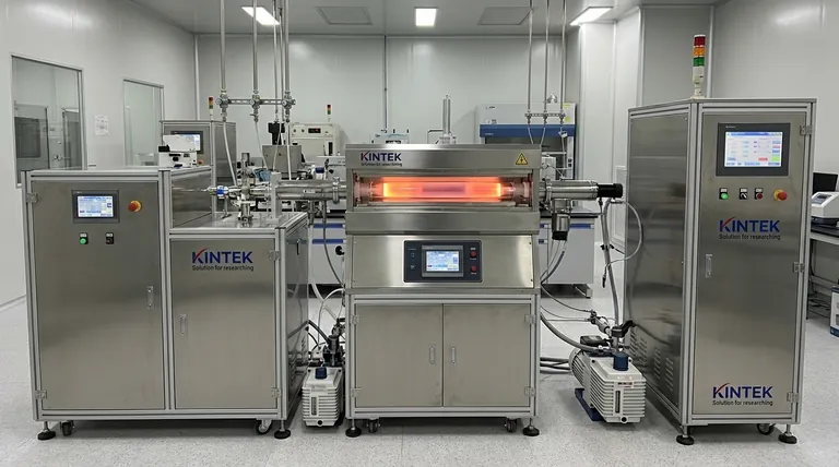
Visual Guide
Related Products
- Slide PECVD Tube Furnace with Liquid Gasifier PECVD Machine
- RF PECVD System Radio Frequency Plasma Enhanced Chemical Vapor Deposition
- Inclined Rotary Plasma Enhanced Chemical Deposition PECVD Tube Furnace Machine
- Inclined Rotary Plasma Enhanced Chemical Deposition PECVD Tube Furnace Machine
- Multi Heating Zones CVD Tube Furnace Machine for Chemical Vapor Deposition Equipment
People Also Ask
- How does a hydrogen reduction environment in an industrial tube furnace facilitate gold-copper alloy microspheres?
- What are the main advantages of PECVD tube furnaces compared to CVD tube furnaces? Lower Temp, Faster Deposition, and More
- In which industries is the tube furnace commonly used? Essential for Materials Science, Energy, and More
- What are the advantages of using a tube furnace CVD system for Cu(111)/graphene? Superior Scalability and Quality
- What plasma source is used in PE-CVD tube furnaces? Unlock Low-Temperature, High-Quality Deposition


