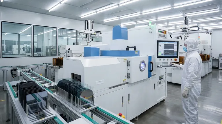
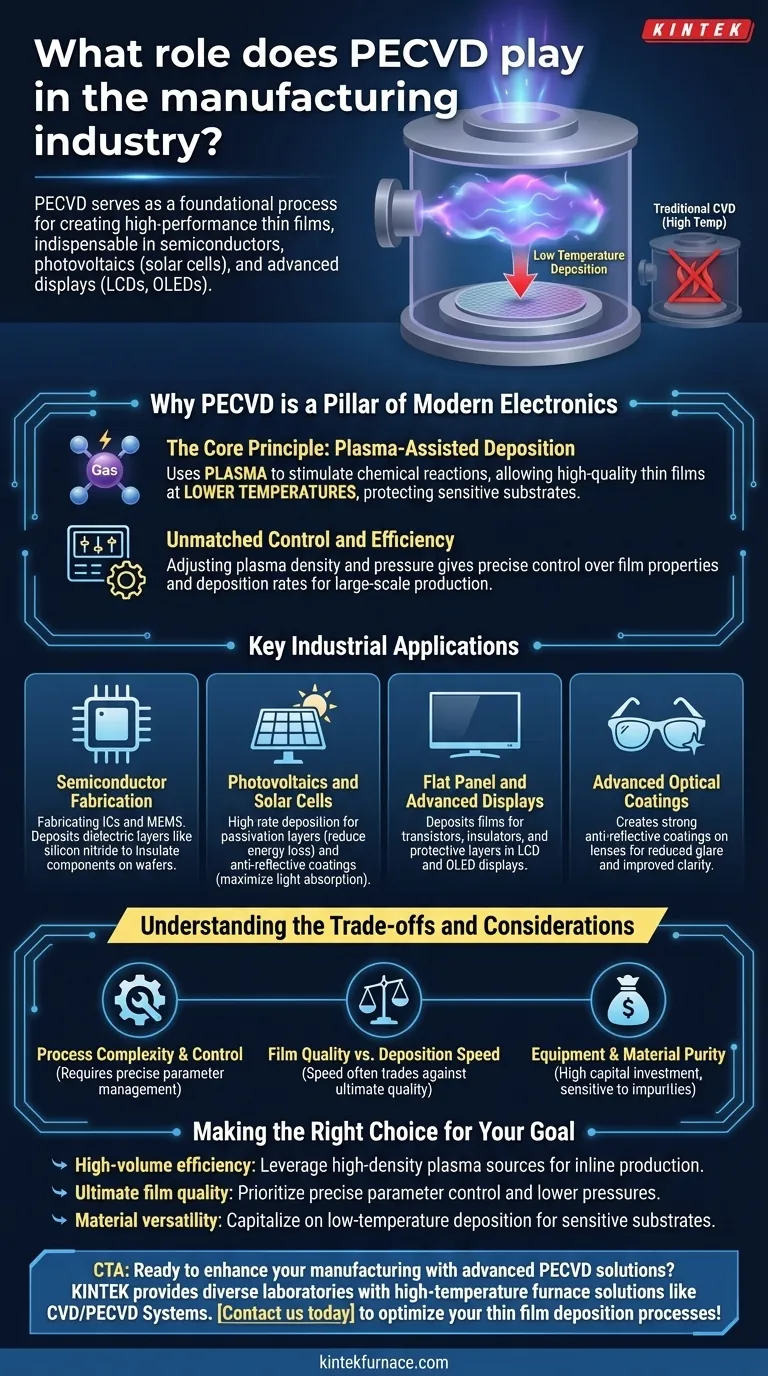
In modern manufacturing, Plasma-Enhanced Chemical Vapor Deposition (PECVD) serves as a foundational process for creating high-performance thin films. It is indispensable in the production of semiconductors, photovoltaics like solar cells, and advanced displays such as LCDs and OLEDs. This technology enables the deposition of precise, uniform layers that are critical to the function of these complex devices.
PECVD's essential role is not just in depositing materials, but in doing so at low temperatures. This single advantage unlocks the ability to manufacture sophisticated electronic components on a massive scale without damaging the underlying sensitive materials.
Why PECVD is a Pillar of Modern Electronics
To understand PECVD's role, you must first understand its core advantage over traditional methods. It solves a fundamental manufacturing challenge: adding high-quality layers to a material without destroying it with heat.
The Core Principle: Plasma-Assisted Deposition
PECVD uses an energized gas, or plasma, to stimulate the chemical reactions needed for deposition.
This plasma creates highly reactive chemical species at a fraction of the thermal energy required by conventional Chemical Vapor Deposition (CVD).
The result is the ability to deposit durable, high-purity thin films at much lower temperatures, protecting the delicate substrates used in semiconductors and displays.
Unmatched Control and Efficiency
Increasing the plasma density raises the concentration of reactive species, which accelerates the deposition rate.
This also allows the process to operate at lower pressures, giving engineers greater control over the direction and energy of ions hitting the substrate surface.
This level of control makes the process both flexible and highly efficient for large-scale production runs.
Key Industrial Applications
PECVD is not a niche technology; it is a versatile platform enabling multiple billion-dollar industries. Its impact is seen in the devices we use every day.
Semiconductor Fabrication
PECVD is a workhorse in fabricating integrated circuits (ICs) and microelectromechanical systems (MEMS). It's used to deposit dielectric layers, such as silicon nitride and silicon dioxide, which insulate components on a silicon wafer.
Photovoltaics and Solar Cells
In the solar industry, efficiency is everything. PECVD is used for high-rate, inline deposition of critical layers on crystalline silicon cells.
These include passivation layers that reduce energy loss and anti-reflective coatings that maximize the amount of light absorbed by the cell.
Flat Panel and Advanced Displays
Modern LCD and OLED displays rely on thin films to function. PECVD deposits films that form transistors, insulators, and protective layers, directly enhancing the performance and longevity of the display.
Advanced Optical Coatings
The same principles apply to optics. PECVD is used to create strong anti-reflective coatings on surfaces like sunglasses and high-end lenses, reducing glare and improving visual clarity.
Understanding the Trade-offs and Considerations
While powerful, PECVD is a sophisticated process with inherent complexities that must be managed for successful implementation.
Process Complexity and Control
Managing a stable plasma requires precise control over gas flow, pressure, power, and frequency. Deviations can impact film uniformity and quality, demanding robust process control systems.
Film Quality vs. Deposition Speed
There is often a trade-off between the speed of deposition and the ultimate quality of the film. High-rate processes, while efficient for volume production, may introduce stresses or impurities that must be carefully characterized and controlled.
Equipment and Material Purity
PECVD systems are significant capital investments. Furthermore, the process is highly sensitive to impurities in source gases, requiring stringent material handling and supply chain management to ensure consistent results.
Making the Right Choice for Your Goal
Applying PECVD effectively means aligning its capabilities with your primary manufacturing objective.
- If your primary focus is high-volume efficiency: Leverage high-density plasma sources, such as Inductively Coupled Plasma (ICP), to achieve the high deposition rates needed for inline production of solar cells or large-area displays.
- If your primary focus is ultimate film quality: Prioritize precise control over plasma parameters and operate at lower pressures to fine-tune film properties like density, stress, and stoichiometry for advanced semiconductors.
- If your primary focus is material versatility: Capitalize on PECVD's low-temperature advantage to deposit films on temperature-sensitive substrates like polymers or pre-fabricated electronic assemblies.
Ultimately, mastering PECVD is about translating atomic-level control into large-scale manufacturing success.
Summary Table:
| Aspect | Details |
|---|---|
| Core Advantage | Low-temperature deposition protects sensitive substrates |
| Key Applications | Semiconductors, photovoltaics, displays, optical coatings |
| Benefits | Precise control, high efficiency, versatility for large-scale production |
| Considerations | Process complexity, trade-offs in speed vs. quality, equipment investment |
Ready to enhance your manufacturing with advanced PECVD solutions? Leveraging exceptional R&D and in-house manufacturing, KINTEK provides diverse laboratories with high-temperature furnace solutions like CVD/PECVD Systems. Our strong deep customization capability ensures precise alignment with your unique experimental needs for semiconductors, solar cells, and displays. Contact us today to discuss how we can optimize your thin film deposition processes and drive your success!
Visual Guide
Related Products
- Slide PECVD Tube Furnace with Liquid Gasifier PECVD Machine
- RF PECVD System Radio Frequency Plasma Enhanced Chemical Vapor Deposition
- Inclined Rotary Plasma Enhanced Chemical Deposition PECVD Tube Furnace Machine
- Inclined Rotary Plasma Enhanced Chemical Deposition PECVD Tube Furnace Machine
- Multi Heating Zones CVD Tube Furnace Machine for Chemical Vapor Deposition Equipment
People Also Ask
- What are the advantages of using a tube furnace CVD system for Cu(111)/graphene? Superior Scalability and Quality
- In which industries is the tube furnace commonly used? Essential for Materials Science, Energy, and More
- What role does a Tube Furnace play in the CVD growth of carbon nanotubes? Achieve High-Purity CNT Synthesis
- What are the main advantages of PECVD tube furnaces compared to CVD tube furnaces? Lower Temp, Faster Deposition, and More
- What are the disadvantages of tube furnace cracking when processing heavy raw materials? Avoid Costly Downtime and Inefficiency


