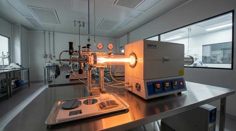
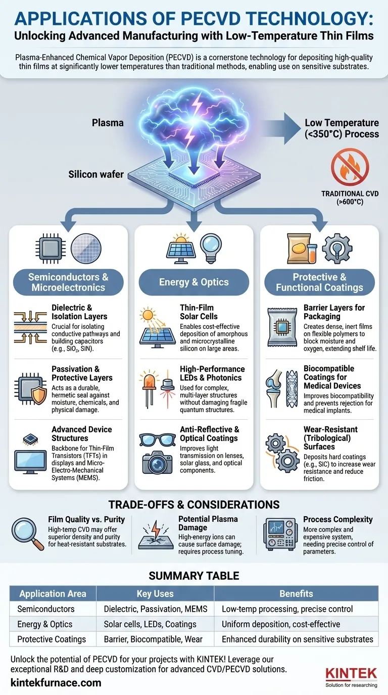
At its core, Plasma-Enhanced Chemical Vapor Deposition (PECVD) is a cornerstone technology for modern manufacturing, primarily used to deposit thin films onto substrates that cannot withstand high heat. Its main applications are in fabricating semiconductor devices, producing thin-film solar cells, and creating protective optical and barrier coatings for everything from medical implants to food packaging. The process is valued for its ability to create high-quality, uniform layers at significantly lower temperatures than traditional deposition methods.
The central challenge in modern device fabrication is applying high-performance thin films without damaging the underlying, often delicate, material. PECVD solves this by using an energy-rich plasma, rather than intense heat, to drive chemical reactions, making it the default choice for manufacturing on temperature-sensitive substrates like silicon wafers with existing circuits, plastics, and glass.
The Core Principle: Why Low Temperature is a Game-Changer
To understand PECVD's applications, you must first understand its fundamental advantage over its predecessor, Chemical Vapor Deposition (CVD).
### The High-Heat Problem of Traditional CVD
Traditional CVD requires extremely high temperatures (often >600°C) to provide the thermal energy needed for precursor gases to react and form a solid film. This process works well for robust substrates but will damage or destroy most modern electronic components, polymers, and other advanced materials.
### How Plasma Changes the Equation
PECVD circumvents the need for high heat by introducing energy in a different form: an electromagnetic field that ignites a plasma. This plasma—an energized state of gas—is filled with reactive ions and radicals that can deposit as a high-quality film at much lower temperatures, typically below 350°C.
### The Benefit of Precise Control
Because it relies on plasma instead of heat, PECVD allows for precise control over film properties like thickness, density, and chemical composition. This makes it indispensable for building the complex, multi-layered structures found in modern electronics.
Key Application Sector: Semiconductors and Microelectronics
PECVD is mission-critical in the semiconductor industry. A modern integrated circuit may undergo dozens of PECVD steps during its fabrication.
### Dielectric and Isolation Layers
The most common use of PECVD is depositing dielectric (electrically insulating) films like silicon dioxide (SiO₂) and silicon nitride (SiN). These layers are essential for isolating conductive pathways and building capacitors directly on a silicon wafer.
### Passivation and Protective Layers
Once a chip is fabricated, a final passivation layer of SiN is often applied using PECVD. This layer acts as a durable, hermetic seal that protects the sensitive circuitry from moisture, chemicals, and physical damage.
### Advanced Device Structures
The technology is also crucial for building Thin-Film Transistors (TFTs), which are the backbone of modern displays, and for fabricating Micro-Electro-Mechanical Systems (MEMS), which are tiny sensors and actuators used in everything from smartphones to cars.
Key Application Sector: Energy and Optics
PECVD's ability to deposit uniform films over large areas makes it ideal for manufacturing energy and optical devices.
### Thin-Film Solar Cells
The technology is widely used to create amorphous silicon and microcrystalline silicon thin-film solar cells. PECVD enables cost-effective deposition on large, inexpensive substrates, which is critical for making solar power more accessible.
### High-Performance LEDs and Photonics
Manufacturing high-brightness LEDs and other photonic components like VCSELs involves building complex, multi-layer structures. PECVD allows these layers to be deposited with high precision without damaging the fragile quantum structures that produce light.
### Anti-Reflective and Optical Coatings
PECVD is used to apply anti-reflective coatings to eyeglass lenses, camera lenses, and solar glass, improving light transmission and performance.
Understanding the Trade-offs
While incredibly versatile, PECVD is not a universal solution. Understanding its limitations is key to making informed engineering decisions.
### Film Quality and Purity
For applications where absolute film purity and density are paramount and the substrate is temperature-resistant (like a bare silicon wafer), high-temperature thermal CVD may produce a superior film. PECVD films can sometimes have hydrogen incorporated from precursor gases, which can affect certain electrical properties.
### Potential for Plasma Damage
The high-energy ions within the plasma can sometimes cause physical damage to the substrate surface. While this can be mitigated through process tuning, it remains a consideration for extremely sensitive materials.
### Process Complexity
A PECVD system is more complex and expensive than some alternative deposition methods like sputtering. It requires sophisticated control of gas flow, pressure, power, and temperature to achieve repeatable results.
Key Application Sector: Protective and Functional Coatings
The low-temperature nature of PECVD has opened up its use far beyond electronics, particularly for coating polymers and plastics.
### Barrier Layers for Packaging
PECVD can deposit a dense, inert film on flexible polymer substrates. This is used in food packaging (like the inside of a chip bag) to create a barrier against moisture and oxygen, extending shelf life.
### Biocompatible Coatings for Medical Devices
The surfaces of medical implants can be coated using PECVD to improve their biocompatibility and prevent rejection by the body. These functional coatings can also add wear resistance to artificial joints.
### Wear-Resistant (Tribological) Surfaces
Hard coatings like silicon carbide (SiC) can be deposited via PECVD onto mechanical parts to increase wear resistance and reduce friction, extending the operational life of the component.
How to Apply This to Your Project
Your choice of deposition technology depends entirely on your substrate and desired film properties.
- If your primary focus is cutting-edge microelectronics: PECVD is non-negotiable for depositing dielectric and passivation films onto completed wafers without damaging existing circuits.
- If your primary focus is high-efficiency solar or LEDs: PECVD is the industry standard for creating the necessary complex, multi-layered structures on temperature-sensitive materials.
- If your primary focus is coating flexible polymers or plastics: PECVD is often the only viable high-performance method due to its essential low-temperature processing capability.
- If your primary focus is maximum film purity on a heat-proof substrate: You should also evaluate high-temperature thermal CVD as a potential alternative for its superior film density in specific cases.
Understanding that PECVD's power lies in decoupling the deposition reaction from high heat is the key to deploying it effectively.
Summary Table:
| Application Area | Key Uses | Benefits |
|---|---|---|
| Semiconductors | Dielectric layers, passivation, MEMS | Low-temperature processing, precise control |
| Energy & Optics | Solar cells, LEDs, anti-reflective coatings | Uniform deposition, cost-effective for large areas |
| Protective Coatings | Barrier layers, biocompatible coatings, wear resistance | Enhanced durability and functionality on sensitive substrates |
Unlock the potential of PECVD for your projects with KINTEK! Leveraging exceptional R&D and in-house manufacturing, we provide advanced high-temperature furnace solutions, including our CVD/PECVD Systems, tailored for diverse laboratories. Our strong deep customization capability ensures precise alignment with your unique experimental needs, whether you're in semiconductors, energy, or protective coatings. Contact us today to discuss how our expertise can enhance your thin-film deposition processes and drive innovation in your industry!
Visual Guide
Related Products
- Slide PECVD Tube Furnace with Liquid Gasifier PECVD Machine
- RF PECVD System Radio Frequency Plasma Enhanced Chemical Vapor Deposition
- Inclined Rotary Plasma Enhanced Chemical Deposition PECVD Tube Furnace Machine
- Inclined Rotary Plasma Enhanced Chemical Deposition PECVD Tube Furnace Machine
- Multi Heating Zones CVD Tube Furnace Machine for Chemical Vapor Deposition Equipment
People Also Ask
- What plasma source is used in PE-CVD tube furnaces? Unlock Low-Temperature, High-Quality Deposition
- What is plasma in the context of PECVD? Unlock Low-Temperature Thin Film Deposition
- What are the main advantages of PECVD tube furnaces compared to CVD tube furnaces? Lower Temp, Faster Deposition, and More
- What are the typical conditions for plasma-enhanced CVD processes? Achieve Low-Temperature Thin Film Deposition
- How does a hydrogen reduction environment in an industrial tube furnace facilitate gold-copper alloy microspheres?


