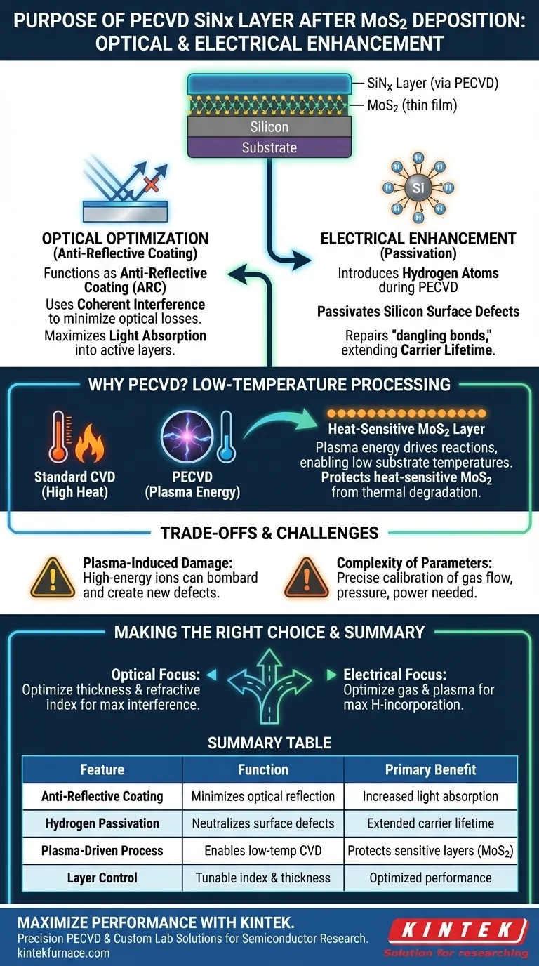
The application of a Silicon Nitride (SiNx) layer via PECVD serves two critical functions: optical optimization and electrical passivation. Specifically, this layer acts as an anti-reflective coating to minimize optical losses while simultaneously introducing hydrogen atoms to passivate the underlying silicon surface, thereby repairing defects.
Core Insight: The value of the SiNx layer is not just structural; it is functional. It leverages coherent interference to capture more light and utilizes hydrogen atoms generated during the PECVD process to neutralize atomic defects, significantly extending the lifespan of charge carriers.
Optical Optimization: Maximizing Light Absorption
The first major purpose of the SiNx layer is to manage how light interacts with the device surface.
Reducing Optical Losses
The SiNx layer functions as a highly effective Anti-Reflective Coating (ARC). By carefully controlling the thickness and refractive index of the SiNx, the layer induces coherent interference.
This optical phenomenon cancels out reflected light waves, ensuring that a higher percentage of incident light reaches the active layers of the device rather than bouncing off the surface.
Electrical Enhancement: The Power of Passivation
The second, and perhaps more nuanced, purpose relates to the chemical interaction between the layer and the substrate.
The Role of Hydrogen
During the PECVD process, hydrogen atoms are naturally introduced into the deposition environment. This is a distinct advantage of using PECVD over other deposition methods that might not introduce hydrogen as effectively.
Repairing Interface Defects
These hydrogen atoms diffuse to the interface where they passivate the silicon surface.
At the atomic level, the hydrogen bonds with "dangling bonds" or defects on the silicon surface. This repair process drastically reduces recombination centers, leading to a significant enhancement in carrier lifetime.
Why PECVD is the Chosen Method
While the SiNx material provides the properties, the PECVD method provides the processing environment necessary to apply it correctly.
Enabling Low-Temperature Processing
Standard Chemical Vapor Deposition (CVD) often requires high temperatures to drive chemical reactions.
PECVD uses plasma energy to drive these reactions instead of heat. This allows the SiNx layer to be deposited at relatively low substrate temperatures, which is critical for protecting heat-sensitive underlying layers (such as MoS2 or other thin films) from thermal degradation.
Understanding the Trade-offs
While PECVD offers significant advantages for passivation and optical tuning, it introduces specific challenges that must be managed.
Plasma-Induced Damage
The same plasma that lowers the processing temperature contains high-energy ions. If not carefully controlled, the glow discharge can bombard the substrate surface, potentially creating new defects even as the hydrogen attempts to repair existing ones.
Complexity of Parameters
PECVD is a complex process involving gas flow rates, pressure, temperature, and plasma power. Achieving the perfect balance between a dense, high-quality SiNx film and effective hydrogen passivation requires precise calibration of these variables.
Making the Right Choice for Your Goal
The effectiveness of the SiNx layer depends on tuning the PECVD parameters to match your specific performance metrics.
- If your primary focus is Optical Efficiency: Prioritize the precise control of film thickness and refractive index to maximize destructive interference of reflected light.
- If your primary focus is Electrical Performance: Optimize the gas mixture and plasma conditions to maximize hydrogen incorporation for superior defect passivation and carrier lifetime.
Ultimately, the SiNx layer transforms the device surface from a passive interface into an active component that boosts both light capture and electrical efficiency.
Summary Table:
| Feature | Function | Primary Benefit |
|---|---|---|
| Anti-Reflective Coating | Minimizes optical reflection via coherent interference | Increased light absorption and efficiency |
| Hydrogen Passivation | Neutralizes dangling bonds and surface defects | Extended carrier lifetime and electrical stability |
| Plasma-Driven Process | Enables low-temperature chemical vapor deposition | Protects heat-sensitive layers like MoS2 from damage |
| Layer Control | Tunable refractive index and film thickness | Optimized performance for specific device needs |
Maximize Your Material Performance with KINTEK
Precision matters when depositing critical layers like SiNx for your semiconductor research. Backed by expert R&D and manufacturing, KINTEK offers high-performance CVD, PECVD, and vacuum systems specifically designed to provide the precise plasma control and temperature stability your projects demand. Whether you are working with MoS2 or other sensitive thin films, our customizable lab solutions ensure optimal passivation and optical tuning for your unique needs.
Ready to elevate your lab's capabilities? Contact KINTEK today to discuss your custom furnace and deposition requirements with our specialists.
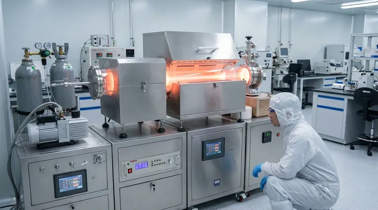
Visual Guide
References
- Sel Gi Ryu, Keunjoo Kim. Photoenhanced Galvanic Effect on Carrier Collection of the MOS<sub>2</sub> Contact Layer in Silicon Solar Cells. DOI: 10.1002/pssa.202500039
This article is also based on technical information from Kintek Furnace Knowledge Base .
Related Products
- RF PECVD System Radio Frequency Plasma Enhanced Chemical Vapor Deposition
- Slide PECVD Tube Furnace with Liquid Gasifier PECVD Machine
- Inclined Rotary Plasma Enhanced Chemical Deposition PECVD Tube Furnace Machine
- Inclined Rotary Plasma Enhanced Chemical Deposition PECVD Tube Furnace Machine
- 915MHz MPCVD Diamond Machine Microwave Plasma Chemical Vapor Deposition System Reactor
People Also Ask
- What are the system specifications of the PECVD system? Unlock Precision Thin-Film Deposition
- What are the applications of plasma enhanced chemical vapor deposition? Key Uses in Electronics, Optics & Materials
- What is the role of RF power in PECVD and how does the RF-PECVD process work? Master Thin Film Deposition Control
- What are the limitations of PECVD? Overcome Process Control and Cost Challenges
- What are some promising applications of PECVD-prepared 2D materials? Unlock Advanced Sensing and Optoelectronics


