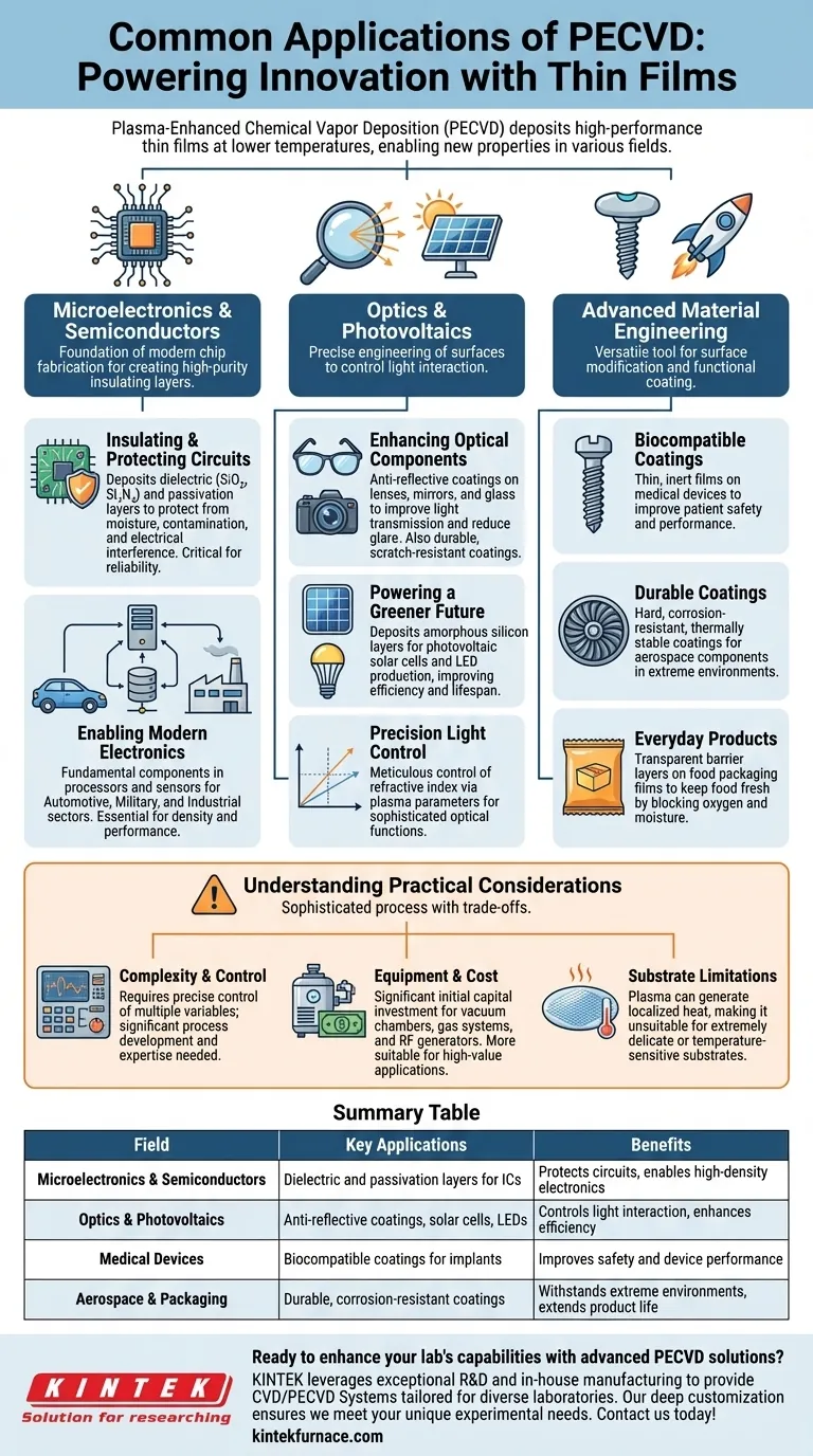
At its core, Plasma-Enhanced Chemical Vapor Deposition (PECVD) is a foundational technology used across any field that requires high-performance thin films. Its most common applications are in the microelectronics and semiconductor industries, followed closely by optics, photovoltaics, medical devices, and aerospace for creating specialized surface coatings.
The true value of PECVD is its ability to deposit uniform, high-quality thin films at lower temperatures than traditional methods. This capability allows manufacturers to add new properties—like electrical insulation, optical transparency, or physical durability—to materials that would be damaged by high heat.
The Foundation: Microelectronics and Semiconductors
PECVD is the workhorse of the modern semiconductor fabrication plant. Its ability to create high-purity insulating layers at relatively low temperatures is essential for building complex, multi-layered integrated circuits.
Insulating and Protecting Circuits
The primary use of PECVD in this field is to deposit dielectric (electrically insulating) and passivation layers. These films, such as silicon dioxide (SiO₂) and silicon nitride (Si₃N₄), protect the sensitive electronic components from moisture, contamination, and electrical interference.
This protective function is critical for the reliability and longevity of microchips.
Enabling Modern Electronics
The chips and circuits enabled by PECVD are fundamental components in nearly every advanced electronic system. This includes the processors and sensors found in the automotive, military, and industrial sectors.
Without these high-quality insulating films, the density and performance of modern microelectronics would not be possible.
Shaping Light: Optics and Photovoltaics
PECVD allows for the precise engineering of a material's surface to control how it interacts with light. This has made it an indispensable tool in both consumer and industrial optics.
Enhancing Optical Components
Thin films are applied to lenses, mirrors, and glass to create specific properties. Anti-reflective coatings on eyeglasses and camera lenses, for example, are a common application that improves light transmission and reduces glare.
Other coatings can enhance reflectivity for mirrors or provide a durable, scratch-resistant surface.
Powering a Greener Future
The technology is instrumental in manufacturing photovoltaic solar cells. PECVD is used to deposit the critical layers of amorphous silicon that convert sunlight into electricity.
It is also used in the production of LEDs, contributing to the efficiency and lifespan of modern lighting.
Precision Control of Light
The key advantage of PECVD in optics is the ability to meticulously control the refractive index of the deposited film. By adjusting plasma parameters like gas composition and pressure, engineers can fine-tune a coating for a specific optical function.
This level of control is necessary for sophisticated devices like optical data storage systems and scientific photometers.
Advanced Material and Surface Engineering
Beyond electronics and optics, PECVD is a versatile tool for enhancing the physical properties of a surface. This is often referred to as surface modification or functional coating.
Biocompatible Coatings for Medical Devices
PECVD can apply thin, inert films to medical implants and tools. These biocompatible coatings prevent the device from reacting with the body, improving patient safety and device performance.
Durable Coatings for Extreme Environments
In the aerospace industry, PECVD is used to apply hard, corrosion-resistant, and thermally stable coatings to components that must withstand extreme conditions.
Improving Everyday Products
The technology has even found use in large-scale applications like the food packaging industry. PECVD can create thin, transparent barrier layers on plastic films, improving their ability to keep food fresh by blocking oxygen and moisture.
Understanding the Practical Considerations
While powerful, PECVD is a sophisticated process with specific trade-offs that determine its suitability for a given application.
Complexity and Control
Achieving a uniform, high-quality film requires precise control over numerous variables, including gas flow rates, pressure, temperature, and plasma power. This complexity means that significant process development and expertise are required.
Equipment and Cost
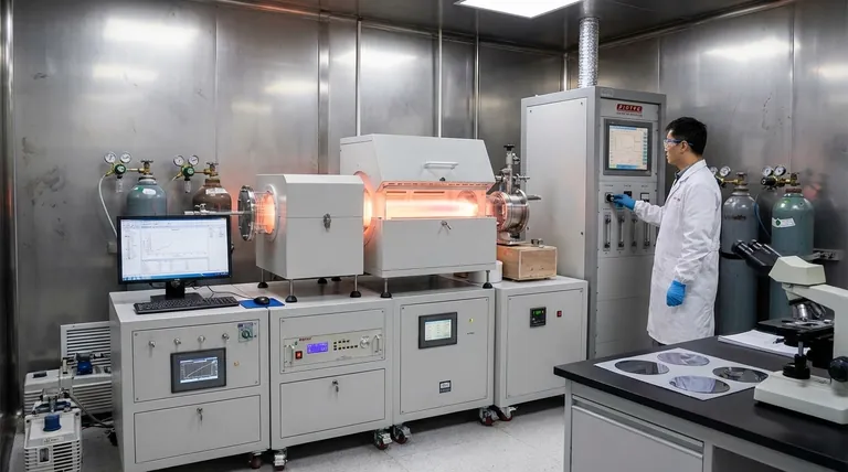
PECVD systems involve vacuum chambers, gas delivery systems, and RF power generators, making the initial capital investment significant. This generally makes it more suitable for high-value applications rather than low-cost bulk material treatment.
Substrate Limitations
Although PECVD is a "low-temperature" process compared to conventional CVD, the plasma can still generate localized heat. This can make it unsuitable for extremely delicate or temperature-sensitive substrates that might deform or outgas during deposition.
Making the Right Choice for Your Goal
To determine if PECVD is the right technology, consider the fundamental property you need to achieve.
- If your primary focus is electronic device fabrication: PECVD is the industry standard for depositing the critical insulating and protective thin films that make modern chips possible.
- If your primary focus is optical performance: Use PECVD for its unparalleled ability to fine-tune a material's refractive index for creating anti-reflection, high-reflectivity, or filter coatings.
- If your primary focus is surface protection or biocompatibility: PECVD provides an effective method to apply highly durable, functional, or inert coatings without damaging the underlying bulk material.
Ultimately, PECVD is the technology of choice whenever a material's surface needs to be fundamentally transformed to perform a new function.
Summary Table:
| Field | Key Applications | Benefits |
|---|---|---|
| Microelectronics & Semiconductors | Dielectric and passivation layers for ICs | Protects circuits, enables high-density electronics |
| Optics & Photovoltaics | Anti-reflective coatings, solar cells, LEDs | Controls light interaction, enhances efficiency |
| Medical Devices | Biocompatible coatings for implants | Improves safety and device performance |
| Aerospace & Packaging | Durable, corrosion-resistant coatings | Withstands extreme environments, extends product life |
Ready to enhance your lab's capabilities with advanced PECVD solutions? KINTEK leverages exceptional R&D and in-house manufacturing to provide high-temperature furnace systems, including CVD/PECVD Systems, tailored for diverse laboratories. Our deep customization ensures we meet your unique experimental needs—contact us today to discuss how we can drive your innovations forward!
Visual Guide
Related Products
- Slide PECVD Tube Furnace with Liquid Gasifier PECVD Machine
- RF PECVD System Radio Frequency Plasma Enhanced Chemical Vapor Deposition
- Inclined Rotary Plasma Enhanced Chemical Deposition PECVD Tube Furnace Machine
- Inclined Rotary Plasma Enhanced Chemical Deposition PECVD Tube Furnace Machine
- Multi Heating Zones CVD Tube Furnace Machine for Chemical Vapor Deposition Equipment
People Also Ask
- What is plasma in the context of PECVD? Unlock Low-Temperature Thin Film Deposition
- What are the disadvantages of tube furnace cracking when processing heavy raw materials? Avoid Costly Downtime and Inefficiency
- What are the typical conditions for plasma-enhanced CVD processes? Achieve Low-Temperature Thin Film Deposition
- How does PECVD equipment contribute to TOPCon bottom cells? Mastering Hydrogenation for Maximum Solar Efficiency
- What are the advantages of using a tube furnace CVD system for Cu(111)/graphene? Superior Scalability and Quality


