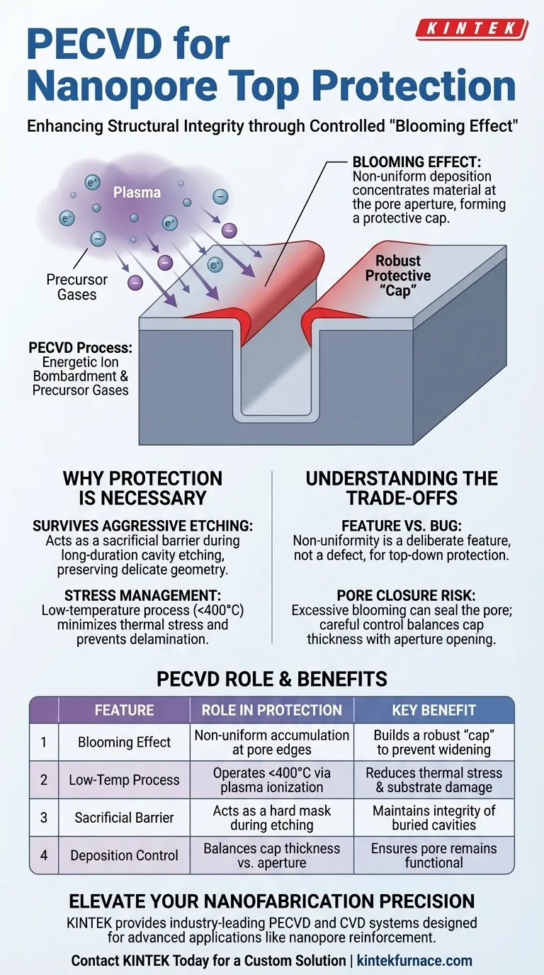
Plasma Enhanced Chemical Vapor Deposition (PECVD) primarily serves as a structural reinforcement mechanism for nanopores by intentionally creating a robust "cap" at the pore's opening. Unlike standard deposition techniques where perfect uniformity is often the goal, this application leverages the "blooming effect"—a non-uniform deposition characteristic—to build up a thicker oxide layer specifically at the top corners of the pore edges.
Core Takeaway: The value of PECVD in this context lies in its specific non-uniformity. By generating a "blooming effect," the system concentrates material accumulation at the pore aperture, creating a protective cap that prevents membrane fracture and unintended pore widening during subsequent aggressive etching processes.
The Mechanics of Top Protection
Utilizing the Blooming Effect
The primary mechanism for enhancing top protection is a phenomenon known as the blooming effect. During the deposition process, the PECVD system creates a non-uniform accumulation of material.
The system deposits a significantly thicker layer of oxide at the top corners of the nanopore compared to the sidewalls or the bottom. This results in an overhang or "cap-like" structure that effectively shields the vulnerable edges of the pore.
Preventing Structural Degradation
This reinforced cap is essential for maintaining the integrity of the nanopore. Without this specialized top protection, the edges of the pore would be susceptible to erosion.
Specifically, the cap prevents the top-layer membrane from breaking and stops the pore diameter from expanding. This structural rigidity is critical for ensuring the device functions as intended after fabrication.
Why This Protection is Necessary
Surviving Long-Duration Etching
Nanopore fabrication often involves releasing buried cavities beneath the surface layer. This requires long-duration etching processes that are chemically aggressive.
The PECVD-deposited cap acts as a sacrificial barrier or a hard mask during these steps. It ensures that the etchant acts on the cavity below without destroying the delicate geometry of the pore opening above.
Stress Management
The PECVD process operates at relatively low temperatures (generally below 400°C) because the plasma provides the necessary energy for chemical reactions rather than thermal heat.
This low-thermal budget results in films with lower internal stress. A low-stress protective cap is less likely to crack or delaminate from the substrate, further ensuring the reliability of the nanopore protection.
The Deposition Process Context
Plasma Generation and Ionization
To achieve this deposition, the system introduces precursor gases (such as silane and ammonia) into a vacuum chamber. An electric field creates a plasma, ionizing these gases into excited electrons and ions.
Energetic Surface Bombardment
The substrate is bombarded by these energetic ions. This high-energy interaction allows for the precise, albeit non-uniform, buildup of the oxide film.
The specific physics of how these ions arrive at the aperture—often with line-of-sight directionality—contributes to the desired accumulation at the corners (the blooming effect) rather than deep inside the pore.
Understanding the Trade-offs
Non-Uniformity: Feature vs. Bug
In many semiconductor applications, non-uniformity is considered a defect. However, in nanopore protection, it is a deliberate feature.
It is important to recognize that this "blooming" effect limits the system's ability to coat the interior walls of the pore evenly. As the cap grows, it shadows the interior, reducing deposition rates inside the cavity.
Pore Closure Risks
If the deposition process is not carefully controlled, the blooming effect can become too pronounced. This could potentially seal the pore opening entirely before the process is complete.
Operators must balance the need for a thick protective cap with the requirement to keep the nanopore open for its functional purpose.
Making the Right Choice for Your Goal
When integrating PECVD into your fabrication flow, consider your primary constraints:
- If your primary focus is protecting pore geometry during etching: rely on the PECVD "blooming effect" to create a thick, sacrificial cap at the aperture corners.
- If your primary focus is coating the interior sidewalls uniformly: you may need to evaluate Atomic Layer Deposition (ALD) instead, as PECVD is optimized here for top-down line-of-sight protection.
- If your primary focus is substrate preservation: utilize PECVD for its ability to deposit high-quality films at temperatures low enough to prevent thermal damage to sensitive underlying layers.
PECVD transforms the potential liability of non-uniform deposition into a critical asset, shielding delicate nanostructures through strategic material accumulation.
Summary Table:
| Feature | Role in Nanopore Protection | Key Benefit |
|---|---|---|
| Blooming Effect | Creates non-uniform material accumulation at pore edges | Builds a robust 'cap' to prevent widening |
| Low-Temp Process | Operates below 400°C using plasma ionization | Reduces thermal stress and substrate damage |
| Sacrificial Barrier | Acts as a hard mask during long-duration etching | Maintains structural integrity of buried cavities |
| Deposition Control | Balances cap thickness vs. aperture opening | Ensures the pore remains functional and open |
Elevate Your Nanofabrication Precision
Don't let aggressive etching compromise your delicate nanostructures. KINTEK provides industry-leading PECVD and CVD systems specifically designed to give you the control needed for advanced applications like nanopore reinforcement.
Backed by expert R&D and manufacturing, KINTEK offers Muffle, Tube, Rotary, Vacuum, and CVD systems, all customizable for your unique lab needs. Whether you are managing stress in thin films or leveraging the blooming effect for top protection, our technical team is ready to help you optimize your results.
Contact KINTEK Today for a Custom Solution
Visual Guide
References
- Sanjeev Vishal Kota, Henri Jansen. Nano-Perforated Silicon Membrane with Monolithically Integrated Buried Cavity. DOI: 10.3390/mi16010104
This article is also based on technical information from Kintek Furnace Knowledge Base .
Related Products
- RF PECVD System Radio Frequency Plasma Enhanced Chemical Vapor Deposition
- Slide PECVD Tube Furnace with Liquid Gasifier PECVD Machine
- Inclined Rotary Plasma Enhanced Chemical Deposition PECVD Tube Furnace Machine
- Inclined Rotary Plasma Enhanced Chemical Deposition PECVD Tube Furnace Machine
- 915MHz MPCVD Diamond Machine Microwave Plasma Chemical Vapor Deposition System Reactor
People Also Ask
- What are the key advantages of PECVD technology? Achieve Low-Temperature, High-Quality Thin Film Deposition
- What are the applications of plasma enhanced chemical vapor deposition? Key Uses in Electronics, Optics & Materials
- What is PECVD specification? A Guide to Choosing the Right System for Your Lab
- What are some promising applications of PECVD-prepared 2D materials? Unlock Advanced Sensing and Optoelectronics
- What is RF in PECVD? A Critical Control for Plasma Deposition


