At its core, amorphous silicon (a-Si) is suitable for thin-film applications because its disordered atomic structure allows it to be deposited cheaply over large, flexible surfaces at low temperatures. This fundamental property, combined with its strong light absorption, makes it a highly practical material for specific uses like solar cells and display backplanes, even if it doesn't offer the highest electronic performance.
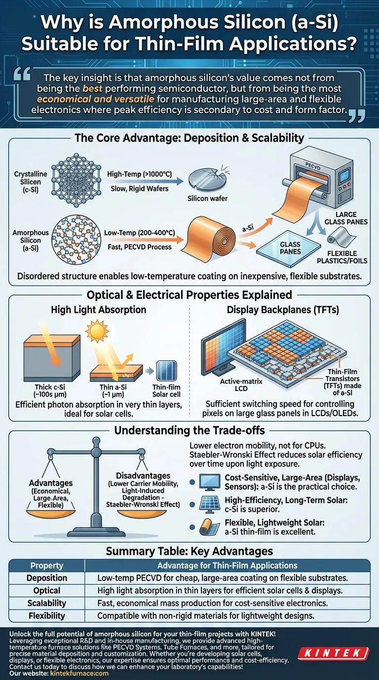
The key insight is that amorphous silicon's value comes not from being the best performing semiconductor, but from being the most economical and versatile for manufacturing large-area and flexible electronics where peak efficiency is secondary to cost and form factor.
The Core Advantage: Deposition and Scalability
The primary distinction between amorphous silicon and its crystalline counterpart is its lack of long-range atomic order. This "disorder" is not a flaw but a feature that fundamentally changes how it can be manufactured.
Overcoming Crystalline Limitations
Crystalline silicon (c-Si), the basis for most computer chips, requires a near-perfect atomic lattice. Growing these crystals is a high-temperature, slow, and expensive process, resulting in rigid, brittle wafers that are difficult to produce in very large sizes.
The Amorphous Advantage: Low-Temperature Processing
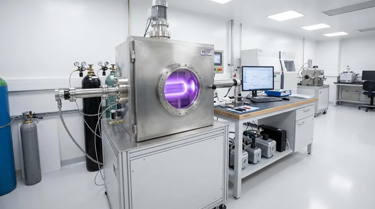
Because a-Si has no crystal structure to perfect, it can be deposited using methods like plasma-enhanced chemical vapor deposition (PECVD) at relatively low temperatures (around 200-400°C). This process is fast, efficient, and highly scalable.
Enabling Flexible and Large-Area Substrates
The low deposition temperature is the critical enabler. It allows a-Si to be coated onto inexpensive substrates like large panes of glass, flexible plastics, or even metal foils without melting or damaging them. This is impossible with high-temperature crystalline silicon processing.
Optical and Electrical Properties Explained
Beyond its manufacturing benefits, a-Si possesses distinct physical properties that make it uniquely suited for specific thin-film roles.
High Light Absorption
The disordered structure of amorphous silicon alters its interaction with light. It absorbs photons, particularly in the visible spectrum, much more efficiently than crystalline silicon. This means a very thin layer of a-Si (around 1 micrometer) can absorb the same amount of sunlight as a much thicker layer of c-Si (hundreds of micrometers), making it ideal for thin-film solar cells.
The Backbone of Modern Displays
Amorphous silicon is the workhorse behind the active-matrix displays in most LCD and many OLED screens. It is used to create the thin-film transistors (TFTs) that act as individual switches for each pixel. While its electron mobility is low, it is sufficient for the switching speeds required to control pixels on a large glass panel, a feat that is not economically viable with crystalline silicon.
Understanding the Trade-offs
The choice to use a-Si is always a matter of balancing its advantages against significant performance compromises. Acknowledging these trade-offs is key to understanding its place in the market.
The Downside of Disorder: Lower Carrier Mobility
The same atomic disorder that simplifies manufacturing also creates defects that impede the flow of electrons. This results in low carrier mobility, meaning a-Si is a poor choice for high-speed processing applications like CPUs, where crystalline silicon's perfect structure is non-negotiable.
The Staebler-Wronski Effect: Light-Induced Degradation
A critical issue for a-Si solar cells is a phenomenon known as the Staebler-Wronski Effect. Upon initial exposure to light, the material's atomic structure changes slightly, creating new defects that reduce the solar cell's power conversion efficiency. This degradation is a well-known trade-off for its low manufacturing cost.
Efficiency vs. Cost
Ultimately, a-Si is chosen for applications where cost-per-area is the dominant metric. For a display manufacturer, the ability to pattern millions of functional transistors on a square meter of glass is paramount. For some solar applications, a lower-cost, flexible panel is more valuable than a rigid, high-efficiency one.
Making the Right Choice for Your Application
The decision to use amorphous silicon hinges entirely on the specific goals of your project.
- If your primary focus is cost-sensitive, large-area electronics like displays or basic sensors: Amorphous silicon's ability to be deposited cheaply on glass makes it the established and most practical choice.
- If your primary focus is high-efficiency, long-term stable solar power: Crystalline or polycrystalline silicon are superior options, despite their higher initial cost and physical rigidity.
- If your primary focus is flexible, lightweight solar power where portability matters more than peak efficiency: Amorphous silicon thin-film cells are an excellent candidate due to their compatibility with plastic or metal substrates.
Choosing the right material requires understanding that engineering is an exercise in managing deliberate trade-offs to meet a specific goal.
Summary Table:
| Property | Advantage for Thin-Film Applications |
|---|---|
| Deposition | Low-temperature PECVD enables cheap, large-area coating on flexible substrates like glass and plastics. |
| Optical | High light absorption in thin layers (∼1 μm) makes it ideal for efficient solar cells and displays. |
| Scalability | Fast, economical manufacturing supports mass production for cost-sensitive electronics. |
| Flexibility | Compatible with non-rigid materials, allowing for lightweight and portable device designs. |
Unlock the full potential of amorphous silicon for your thin-film projects with KINTEK! Leveraging exceptional R&D and in-house manufacturing, we provide advanced high-temperature furnace solutions like PECVD Systems, Tube Furnaces, and more, tailored for precise material deposition and customization. Whether you're developing solar cells, displays, or flexible electronics, our expertise ensures optimal performance and cost-efficiency. Contact us today to discuss how we can enhance your laboratory's capabilities and meet your unique experimental needs!
Visual Guide
Related Products
- HFCVD Machine System Equipment for Drawing Die Nano Diamond Coating
- Custom Made Versatile CVD Tube Furnace Chemical Vapor Deposition CVD Equipment Machine
- Multi Heating Zones CVD Tube Furnace Machine for Chemical Vapor Deposition Equipment
- MPCVD Machine System Reactor Bell-jar Resonator for Lab and Diamond Growth
- 915MHz MPCVD Diamond Machine Microwave Plasma Chemical Vapor Deposition System Reactor
People Also Ask
- What role does Chemical Vapor Deposition (CVD) equipment play in the surface coating of carbon fibers for composites?
- How can customers maximize the quality of CVD coatings? Master Pre-Coating Prep for Superior Results
- What is chemical vapor deposition (CVD) and its primary industrial application? Unlock Precision Thin Films for Electronics
- What is Hot-filament Chemical Vapor Deposition (HFCVD)? Achieve High-Quality Thin Films with Precision Control
- What are the equipment for chemical vapor deposition? A Guide to the 5 Essential Components


