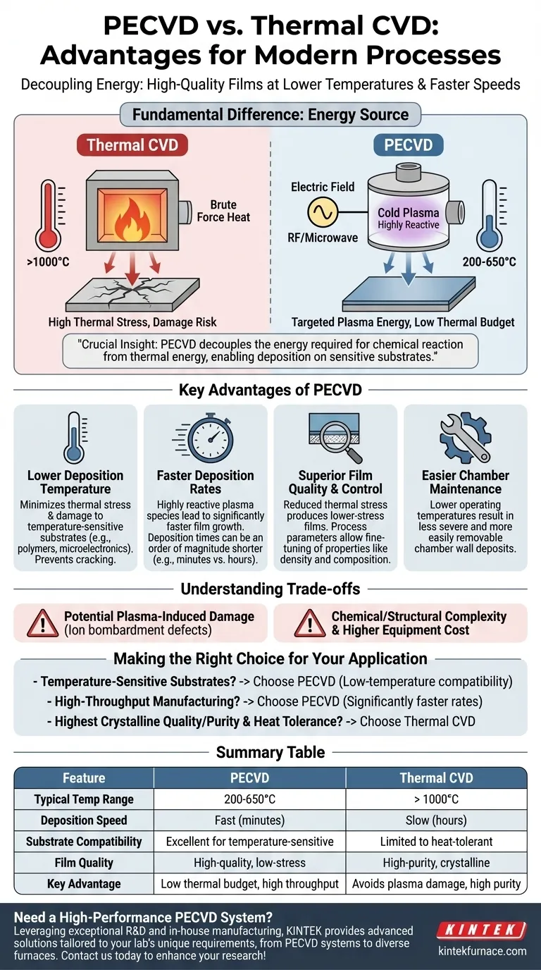
At its core, the primary advantage of Plasma Enhanced Chemical Vapor Deposition (PECVD) is its ability to grow high-quality films at significantly lower temperatures and faster speeds than traditional thermal CVD processes. By using an energized plasma to break down precursor gases instead of relying solely on high heat, PECVD avoids the thermal stress that can damage sensitive substrates or underlying device layers.
The crucial insight is that PECVD decouples the energy required for chemical reaction from thermal energy. This use of "cold plasma" makes it possible to deposit materials on substrates that simply could not survive the extreme temperatures of conventional CVD.
The Fundamental Difference: Energy Source
To understand PECVD's advantages, you must first grasp how it differs from thermal CVD in its method of providing energy for the deposition reaction.
Thermal CVD: Brute Force Heat
Traditional Chemical Vapor Deposition (CVD) is conceptually simple. It uses very high temperatures, often exceeding 1000°C, to give precursor gas molecules enough thermal energy to decompose and react on a substrate surface.
This process is effective but indiscriminate. The high heat affects everything in the chamber, including the substrate and any previously fabricated structures on it.
PECVD: Targeted Plasma Energy
PECVD operates at much lower temperatures, typically in the 200-650°C range. Instead of heat, it uses an electric field (such as radio frequency or microwave) to ionize the precursor gases, creating a plasma.
This plasma is a highly reactive soup of ions, electrons, and radicals. These energized species can then react and deposit on the substrate surface without the need for extreme thermal energy, a state often referred to as "cold plasma."
Key Advantages of PECVD
This fundamental difference in energy delivery leads to several significant operational benefits.
Lower Deposition Temperature
This is the most critical advantage. The ability to deposit films at lower temperatures prevents damage to temperature-sensitive substrates, such as polymers, or delicate microelectronic components already present on a silicon wafer.
It dramatically reduces the thermal budget of the overall fabrication process, minimizing stress and potential cracking in the deposited layers.
Faster Deposition Rates
The highly reactive species in the plasma lead to a more efficient deposition process. This results in significantly faster film growth, with deposition times that can be an order of magnitude shorter than thermal CVD.
For example, a process that might take an hour in a thermal reactor could potentially be completed in around 5 minutes with PECVD, boosting manufacturing throughput.
Superior Film Quality and Control
While seemingly counterintuitive, the low-temperature PECVD process often produces higher-quality films. The reduced thermal stress minimizes the likelihood of cracking.
Furthermore, the plasma parameters (power, pressure, gas flow) give engineers additional "knobs" to tune the properties of the film, such as its density, stress, and composition.
Easier Chamber Maintenance
A practical but important benefit is the ease of chamber cleaning. The lower operating temperatures in a PECVD system generally result in less severe and more easily removable deposits on the chamber walls compared to a high-temperature thermal CVD reactor.
Understanding the Trade-offs
No process is without its compromises. While powerful, PECVD has characteristics that must be considered.
Potential for Plasma-Induced Damage
The same energetic ions that enable low-temperature deposition can also physically bombard the substrate and growing film. This can sometimes introduce defects or damage, a factor that is absent in the purely thermal process.
Chemical and Structural Complexity
The plasma environment can be chemically complex. This can sometimes lead to the unwanted incorporation of elements, such as hydrogen from precursor molecules, into the final film, which can affect its electrical or optical properties. Films are also often amorphous or polycrystalline rather than single-crystal.
Equipment Cost and Complexity
PECVD systems, with their required RF or microwave power generators and impedance-matching networks, are inherently more complex and expensive than the relatively simpler furnaces used for thermal CVD.
Making the Right Choice for Your Application
Selecting the right deposition method depends entirely on the specific requirements of your substrate and final film.
- If your primary focus is working with temperature-sensitive substrates (like polymers, organics, or completed circuits): PECVD is the clear and often only choice due to its low-temperature processing.
- If your primary focus is high-throughput manufacturing and speed: PECVD's significantly faster deposition rates provide a major advantage for production efficiency.
- If your primary focus is achieving the highest possible crystalline quality and purity, and your substrate can tolerate the heat: Thermal CVD or epitaxial processes may be more suitable as they avoid any risk of plasma-induced damage.
Ultimately, your decision hinges on balancing the need for low-temperature compatibility and speed against the unique complexities of a plasma-based process.
Summary Table:
| Feature | PECVD | Thermal CVD |
|---|---|---|
| Typical Temperature Range | 200-650°C | > 1000°C |
| Deposition Speed | Fast (minutes) | Slow (hours) |
| Substrate Compatibility | Excellent for temperature-sensitive materials (e.g., polymers) | Limited to high-temperature tolerant substrates |
| Film Quality | High-quality, low-stress films | High-purity, crystalline films (if substrate tolerates heat) |
| Key Advantage | Low thermal budget, high throughput | Avoids plasma-induced damage, high purity |
Need a High-Performance PECVD System Tailored to Your Lab's Unique Requirements?
Leveraging exceptional R&D and in-house manufacturing, KINTEK provides diverse laboratories with advanced high-temperature furnace solutions. Our PECVD systems are designed to deliver the low-temperature, high-speed deposition capabilities your sensitive substrates demand. Our product line, including Muffle, Tube, Rotary Furnaces, Vacuum & Atmosphere Furnaces, and CVD/PECVD Systems, is complemented by our strong deep customization capability to precisely meet your unique experimental requirements.
Contact us today to discuss how our PECVD solutions can enhance your research and manufacturing processes!
Visual Guide
Related Products
- 915MHz MPCVD Diamond Machine Microwave Plasma Chemical Vapor Deposition System Reactor
- RF PECVD System Radio Frequency Plasma Enhanced Chemical Vapor Deposition
- MPCVD Machine System Reactor Bell-jar Resonator for Lab and Diamond Growth
- Slide PECVD Tube Furnace with Liquid Gasifier PECVD Machine
- Inclined Rotary Plasma Enhanced Chemical Deposition PECVD Tube Furnace Machine
People Also Ask
- What is the basic principle of operation for the microwave plasma chemical vapor deposition system? Unlock High-Purity Material Growth
- What factors influence the quality of diamond deposition in the MPCVD method? Master the Critical Parameters for High-Quality Diamond Growth
- What are some key features and benefits of the microwave plasma chemical vapor deposition system? Achieve Unmatched Material Synthesis
- What are the essential components of an MPCVD reactor for diamond film deposition? Unlock High-Quality Diamond Growth
- What is the MPCVD method and why is it considered effective for diamond deposition? Superior Purity & High Growth Rates


