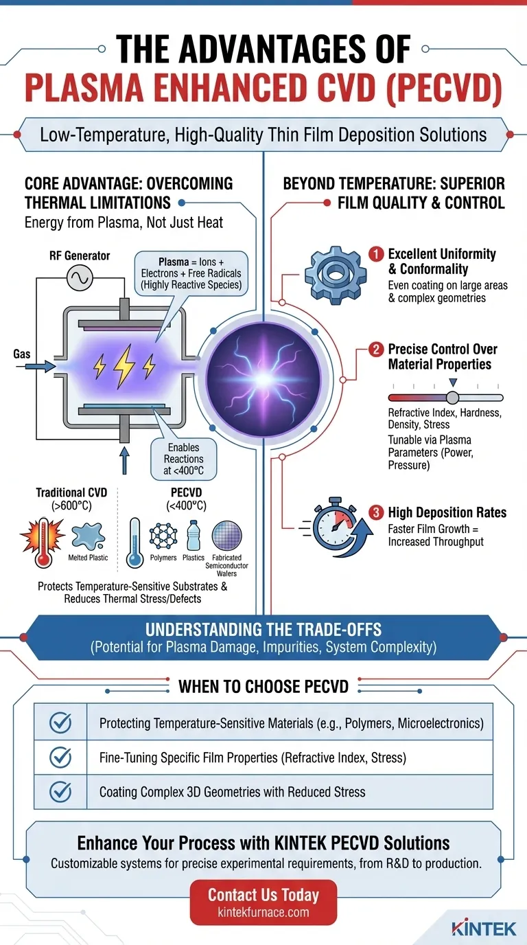
Fundamentally, the key advantage of Plasma-Enhanced Chemical Vapor Deposition (PECVD) is its ability to operate at significantly lower temperatures than traditional Chemical Vapor Deposition (CVD). This is achieved by using an energy-rich plasma to drive the chemical reactions needed to form a thin film, rather than relying solely on high heat. This critical difference allows for the deposition of high-quality films on materials that would otherwise be damaged or destroyed by conventional high-temperature processes.
The central innovation of PECVD is using an energy-rich plasma to supplement or replace thermal energy. This decoupling of the reaction from high heat allows for high-quality film deposition at temperatures low enough to protect sensitive underlying substrates, a capability that traditional CVD cannot offer.
The Core Advantage: Overcoming Thermal Limitations
Traditional CVD requires high temperatures, often exceeding 600°C, to provide enough energy to break down precursor gases and initiate the chemical reaction that forms the film. PECVD bypasses this thermal barrier.
How PECVD Works: Energy from Plasma, Not Just Heat
In a PECVD process, an electrical field (typically radio frequency) is applied to the precursor gas mixture inside a vacuum chamber. This field energizes the gas, stripping electrons from the atoms and creating a plasma—a highly reactive state of matter containing ions, electrons, and free radicals.
These reactive species have enough energy to form the desired film on the substrate surface at much lower temperatures, often below 400°C.
Protecting Temperature-Sensitive Substrates
The most significant benefit of this low-temperature operation is the ability to coat materials that cannot withstand high heat. This opens up applications that are impossible for traditional CVD.
Examples include depositing films on polymers, plastics, or fully fabricated semiconductor wafers that already contain metallic interconnects or other structures with low melting points.
Reducing Thermal Stress and Defects
When a film is deposited at high temperatures, the difference in thermal expansion between the film and the substrate can create significant mechanical stress as the part cools down. This stress can lead to film cracking, delamination, or warping of the substrate.
By operating at lower temperatures, PECVD dramatically reduces this thermally-induced stress, improving film adhesion and overall device reliability.
Beyond Temperature: Superior Film Quality and Control
While lower temperature is the primary driver for adopting PECVD, the use of plasma provides several other distinct advantages related to the quality and precision of the deposited film.
Excellent Film Uniformity and Conformality
The plasma helps distribute the reactive precursor species more evenly throughout the chamber. This results in a highly uniform film thickness across the entire substrate, even over large areas.
This process also provides excellent conformality, meaning it can evenly coat complex, non-flat, or three-dimensional surfaces. This is often referred to as good "step coverage" in the semiconductor industry.
Precise Control Over Material Properties
In PECVD, the film's properties are not just a function of temperature and gas chemistry; they are also heavily influenced by the plasma itself.
By precisely tuning plasma parameters like power, pressure, and frequency, engineers can finely control key material properties. This includes the film's refractive index (critical for optical coatings), hardness, density, and internal mechanical stress.
High Deposition Rates
The highly reactive nature of the species within the plasma can lead to faster film growth compared to other low-temperature deposition techniques. This increases throughput, making the process more efficient for industrial manufacturing.
Understanding the Trade-offs
No technology is without its limitations. Objectivity requires acknowledging the potential downsides of using a plasma-based process.
Potential for Plasma-Induced Damage
The high-energy ions in the plasma can bombard the substrate surface during deposition. While this can sometimes be beneficial (e.g., improving film density), it can also create crystallographic damage or defects in sensitive substrates like silicon wafers.
Film Composition and Purity
PECVD films can sometimes incorporate elements from the precursor gases, most notably hydrogen. While this can be intentionally used to "passivate" defects, it can also be an unwanted impurity if the goal is an extremely pure film. Traditional high-temperature CVD often yields higher-purity films.
System Complexity
PECVD systems require sophisticated hardware, including RF power generators, matching networks, and robust vacuum systems. This can make them more complex and costly to purchase and maintain compared to simpler atmospheric-pressure or thermal CVD reactors.
When to Choose PECVD
Your choice of deposition technology should be guided by the specific requirements of your final product.
- If your primary focus is depositing on temperature-sensitive materials: PECVD is the definitive choice to prevent thermal damage to substrates like polymers, plastics, or complex microelectronics.
- If your primary focus is fine-tuning specific film properties: PECVD offers superior control over refractive index, stress, and density by allowing you to adjust plasma parameters independently of temperature.
- If your primary focus is achieving the highest possible film purity: Traditional high-temperature CVD might be a better option, as it avoids potential hydrogen incorporation and plasma-induced damage.
- If your primary focus is coating complex 3D geometries: Both CVD and PECVD offer excellent conformality, but PECVD achieves this at a lower temperature, which is critical for reducing thermal stress on the part.
Ultimately, selecting PECVD is a strategic decision to leverage plasma energy for low-temperature, highly controlled film deposition on a wider range of materials.
Summary Table:
| Key Advantage | Core Benefit |
|---|---|
| Low-Temperature Operation | Protects polymers, plastics, and pre-fabricated semiconductor wafers from thermal damage. |
| Reduced Thermal Stress | Improves film adhesion and device reliability by minimizing thermal expansion mismatch. |
| Superior Film Uniformity & Conformality | Ensures even coating over large areas and complex 3D geometries. |
| Precise Control Over Film Properties | Tune refractive index, hardness, density, and stress via plasma parameters. |
| High Deposition Rates | Increases manufacturing throughput with faster film growth. |
Ready to enhance your thin film processes with advanced, low-temperature solutions?
At KINTEK, we leverage exceptional R&D and in-house manufacturing to provide diverse laboratories with cutting-edge high-temperature furnace solutions. Our product line, including CVD/PECVD Systems, is complemented by strong deep customization capabilities to precisely meet your unique experimental requirements.
Whether you are working with temperature-sensitive substrates or need precise control over film properties, our experts can help you select or customize the ideal PECVD system for your application.
Contact us today to discuss how our PECVD technology can solve your specific deposition challenges and drive your research or production forward!
Visual Guide
Related Products
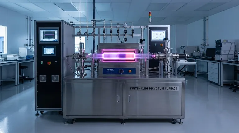
- RF PECVD System Radio Frequency Plasma Enhanced Chemical Vapor Deposition
- Slide PECVD Tube Furnace with Liquid Gasifier PECVD Machine
- Inclined Rotary Plasma Enhanced Chemical Deposition PECVD Tube Furnace Machine
- Inclined Rotary Plasma Enhanced Chemical Deposition PECVD Tube Furnace Machine
- MPCVD Machine System Reactor Bell-jar Resonator for Lab and Diamond Growth
People Also Ask
- What is RF in PECVD? A Critical Control for Plasma Deposition
- What are the key advantages of PECVD technology? Achieve Low-Temperature, High-Quality Thin Film Deposition
- What are the applications of plasma enhanced chemical vapor deposition? Key Uses in Electronics, Optics & Materials
- What are the advantages of PECVD in film deposition? Achieve Low-Temp, High-Quality Coatings
- What is PECVD specification? A Guide to Choosing the Right System for Your Lab