At its core, PECVD achieves superior conformity because it is a diffusive, gas-phase process, unlike the line-of-sight nature of PVD. This fundamental difference in how coating material travels to the substrate allows PECVD to uniformly coat complex, three-dimensional topographies where PVD would leave voids and shadows.
The critical distinction is the transport mechanism. PVD acts like a spray paint can, only coating what it can directly "see." In contrast, PECVD behaves like a fog, with precursor gases filling every crevice of a substrate before reacting to form a film, ensuring even coverage everywhere.
The Fundamental Divide: Gas Diffusion vs. Line-of-Sight
To understand conformity, you must first understand how the coating material arrives at the surface. PVD and PECVD use radically different approaches.
PVD: A Directional, Line-of-Sight Process
Physical Vapor Deposition (PVD) techniques, like sputtering or evaporation, work by physically ejecting or boiling atoms from a solid source material.
These atoms travel in a straight line through a vacuum until they strike the substrate. This is analogous to using a can of spray paint; the paint only lands on the surfaces directly facing the nozzle.
The "Shadowing Effect" in PVD
On an uneven surface with features like trenches or steps, this direct line-of-sight travel creates "shadows."
The tops of features and any surfaces facing the source get a thick coating, while vertical sidewalls and trench bottoms receive very little or no material. This results in poor step coverage and low conformity.
PECVD: A Non-Directional, Diffusive Process
Plasma-Enhanced Chemical Vapor Deposition (PECVD) operates on a completely different principle. It is a chemical, not physical, process.
Precursor gases are introduced into a chamber, where they spread out and diffuse to surround the substrate, much like air filling a room.
An electric field ignites a plasma, which provides the energy to break down these gas molecules into reactive species. These species then adsorb onto the substrate and react to form a solid film.
Why Diffusion Leads to Superior Conformity
The diffusive nature of the PECVD process is the direct cause of its excellent ability to coat complex surfaces uniformly.
Reaching Every Nook and Cranny
Because the precursor gases are not directional, their random motion allows them to penetrate deep into high-aspect-ratio trenches and conform to any shape.
The concentration of the gas becomes relatively uniform across the entire exposed surface area of the substrate, regardless of its orientation.
Deposition via Surface Reaction
The key is that film growth in PECVD is a surface chemical reaction, not just the accumulation of arriving particles.
As long as the reactive precursor gas can reach a surface and the thermal conditions are met, the film will grow there. This ensures that the sidewalls of a trench and its bottom get coated nearly as effectively as the top surface.
Understanding the Trade-offs
While superior for conformity, PECVD is not universally better than PVD. The right choice depends on the specific requirements of the film.
The Case for PVD
Despite its poor conformity, PVD is often preferred for depositing very pure, dense films, particularly metals.
The line-of-sight nature can be an advantage in certain patterning techniques ("lift-off"), and it is generally a faster and simpler process for coating flat surfaces.
Limitations of PECVD
PECVD films are often less dense than PVD films and can contain byproducts from the chemical reaction, such as hydrogen, which may be undesirable.
The process involves more variables (gas flows, pressure, plasma power, temperature), which can make process optimization more complex than for PVD.
Making the Right Choice for Your Application
A true understanding of the material transport mechanism is your best guide for process selection.
- If your primary focus is coating complex 3D structures (e.g., trenches, MEMS): PECVD is the clear choice for its ability to deliver uniform, conformal films at lower temperatures.
- If your primary focus is a high-purity metal film on a flat substrate: PVD offers superior density, purity, and often higher deposition rates.
- If your primary focus is depositing standard dielectrics like silicon nitride or oxide: PECVD is the industry-standard method, offering an excellent balance of conformity and film properties.
By choosing the deposition method based on its fundamental transport physics, you ensure your process is aligned with your design goals from the start.
Summary Table:
| Aspect | PECVD | PVD |
|---|---|---|
| Transport Mechanism | Diffusive, gas-phase | Line-of-sight, directional |
| Conformity on Uneven Surfaces | Excellent, uniform coverage | Poor, shadowing effects |
| Ideal Applications | Complex 3D structures, MEMS, dielectrics | Flat surfaces, high-purity metals |
| Key Advantages | Coats all surfaces, lower temperatures | High density, purity, faster for flat substrates |
Need advanced high-temperature furnace solutions for your lab? KINTEK leverages exceptional R&D and in-house manufacturing to provide tailored CVD/PECVD systems, Muffle, Tube, Rotary, Vacuum & Atmosphere Furnaces. Our deep customization capabilities ensure precise alignment with your unique experimental needs, enhancing conformity and efficiency. Contact us today to discuss how we can support your research and production goals!
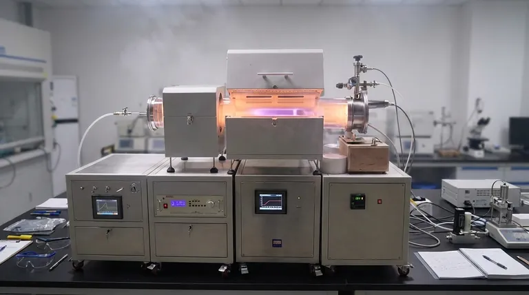
Visual Guide

Related Products
- Slide PECVD Tube Furnace with Liquid Gasifier PECVD Machine
- RF PECVD System Radio Frequency Plasma Enhanced Chemical Vapor Deposition
- Inclined Rotary Plasma Enhanced Chemical Deposition PECVD Tube Furnace Machine
- Inclined Rotary Plasma Enhanced Chemical Deposition PECVD Tube Furnace Machine
- Multi Heating Zones CVD Tube Furnace Machine for Chemical Vapor Deposition Equipment
People Also Ask
- What plasma source is used in PE-CVD tube furnaces? Unlock Low-Temperature, High-Quality Deposition
- What is plasma in the context of PECVD? Unlock Low-Temperature Thin Film Deposition
- What are the typical conditions for plasma-enhanced CVD processes? Achieve Low-Temperature Thin Film Deposition
- In which industries is the tube furnace commonly used? Essential for Materials Science, Energy, and More
- How does a hydrogen reduction environment in an industrial tube furnace facilitate gold-copper alloy microspheres?


