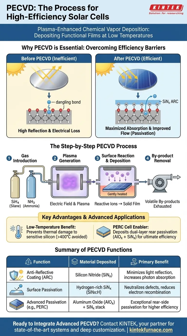
At its core, Plasma-Enhanced Chemical Vapor Deposition (PECVD) is a manufacturing process used to deposit very thin, highly functional films onto solar cells. It works by introducing specific gases into a vacuum chamber, using an electric field to ignite them into a plasma, and allowing the resulting reactive material to form a solid layer on the cell's surface. This process is critical for creating anti-reflective coatings and passivation layers that significantly boost a solar cell's efficiency.
PECVD's primary value in solar cell production is its ability to deposit high-quality films at low temperatures. This allows it to simultaneously reduce light reflection and "heal" electrical defects on the silicon surface, two essential functions for maximizing a cell's power output without damaging the cell itself.
Why PECVD is Essential for Solar Cell Efficiency
The goal of any solar cell is to convert as much sunlight into electricity as possible. PECVD addresses two fundamental barriers to achieving this: light reflection and electrical energy loss.
Enhancing Light Absorption (Anti-Reflective Coating)
A bare silicon wafer is shiny and reflects a significant portion of incoming sunlight. This reflected light is wasted energy.
PECVD is used to deposit a precise layer of silicon nitride (SiNx) on the front surface of the cell. This film acts as an Anti-Reflective Coating (ARC), minimizing reflection and allowing more photons to enter the silicon where they can generate electricity.
Improving Electrical Performance (Surface Passivation)
The surface of a silicon wafer contains microscopic imperfections, often called "dangling bonds." These defects act like traps for the electrons that are freed by sunlight.
When electrons get trapped, they cannot contribute to the electrical current, reducing the cell's overall efficiency. PECVD addresses this by depositing a hydrogen-rich silicon nitride film. The hydrogen atoms in this film bond with and neutralize these surface defects, a process known as passivation. This allows charge carriers to move more freely, boosting the cell's performance.
The Step-by-Step PECVD Process
The PECVD process is a carefully controlled sequence performed inside a specialized vacuum chamber.
Step 1: Gas Introduction
The process begins by feeding precursor gases into the reaction chamber. For creating a silicon nitride layer, these gases are typically silane (SiH4) and ammonia (NH3), often mixed with inert carrier gases.
Step 2: Plasma Generation
A high-frequency electric or magnetic field is applied between two electrodes inside the chamber. This powerful field energizes the gas mixture, stripping electrons from the gas molecules and creating a glowing, ionized gas known as plasma.
This plasma contains highly reactive chemical species, which is the key to why the process can occur at low temperatures.
Step 3: Surface Reaction and Film Deposition
The reactive ions and radicals from the plasma diffuse and land on the surface of the solar cell, which is gently heated. They undergo chemical reactions directly on the surface, bonding together to form a solid, uniform thin film.
Step 4: By-product Removal
The chemical reactions also create volatile by-products. These are continuously pumped out of the vacuum chamber to ensure a pure film is deposited.
Understanding the Key Advantages
The "plasma-enhanced" aspect of PECVD is what gives it a distinct advantage over other deposition methods.
The Critical Role of Low Temperature
Creating silicon nitride through purely thermal methods requires very high temperatures, which can degrade the sensitive electronic properties of the underlying silicon solar cell.
Because the plasma provides the energy needed for the chemical reactions, PECVD can be performed at much lower temperatures (e.g., below 400°C). This allows for the deposition of high-quality films without causing thermal damage to the cell.
Advanced Applications in PERC Cells
Modern high-efficiency cells, like PERC (Passivated Emitter and Rear Cell), rely heavily on PECVD. In these designs, PECVD is used to deposit passivation layers on both the front and rear of the cell.
This often involves a thin layer of aluminum oxide (AlOx) followed by a capping layer of silicon nitride (SiNx:H). This dual-layer structure provides exceptional rear-side passivation, further reducing electrical losses and pushing efficiencies higher.
Making the Right Choice for Your Goal
The application of PECVD is tuned based on the specific performance goal for the solar cell.
- If your primary focus is maximizing light absorption: Use PECVD to deposit a silicon nitride anti-reflective coating with a precisely controlled thickness and refractive index to minimize reflection at key solar wavelengths.
- If your primary focus is boosting electrical efficiency: Use a hydrogen-rich silicon nitride film to achieve excellent surface passivation, reducing carrier recombination at the cell's surface.
- If you are developing advanced cells (like PERC): Employ a multi-step PECVD process to deposit both front-side ARC/passivation layers and rear-side dielectric stacks (AlOx/SiNx) for comprehensive efficiency gains.
Ultimately, PECVD is an indispensable tool that transforms a basic silicon wafer into a high-performance photovoltaic device.
Summary Table:
| PECVD Function | Key Material Deposited | Primary Benefit for Solar Cell |
|---|---|---|
| Anti-Reflective Coating (ARC) | Silicon Nitride (SiNx) | Minimizes light reflection, increases photon absorption |
| Surface Passivation | Hydrogen-rich Silicon Nitride (SiNx:H) | Neutralizes surface defects, reduces electron recombination |
| Advanced Passivation (e.g., PERC) | Aluminum Oxide (AlOx) + SiNx stack | Provides exceptional rear-side passivation for higher efficiency |
Ready to integrate advanced PECVD processes into your solar cell production?
At KINTEK, we leverage our exceptional R&D and in-house manufacturing to provide state-of-the-art PECVD systems and other high-temperature furnace solutions. Our deep customization capabilities ensure our equipment precisely meets your unique research and production requirements for developing next-generation photovoltaic technologies.
Contact our experts today to discuss how our PECVD and CVD systems can optimize your solar cell efficiency and performance.
Visual Guide
Related Products
- Slide PECVD Tube Furnace with Liquid Gasifier PECVD Machine
- RF PECVD System Radio Frequency Plasma Enhanced Chemical Vapor Deposition
- Inclined Rotary Plasma Enhanced Chemical Deposition PECVD Tube Furnace Machine
- Inclined Rotary Plasma Enhanced Chemical Deposition PECVD Tube Furnace Machine
- Multi Heating Zones CVD Tube Furnace Machine for Chemical Vapor Deposition Equipment
People Also Ask
- What are the typical conditions for plasma-enhanced CVD processes? Achieve Low-Temperature Thin Film Deposition
- What role does a Tube Furnace play in the CVD growth of carbon nanotubes? Achieve High-Purity CNT Synthesis
- How does a hydrogen reduction environment in an industrial tube furnace facilitate gold-copper alloy microspheres?
- What plasma source is used in PE-CVD tube furnaces? Unlock Low-Temperature, High-Quality Deposition
- What are the disadvantages of tube furnace cracking when processing heavy raw materials? Avoid Costly Downtime and Inefficiency


