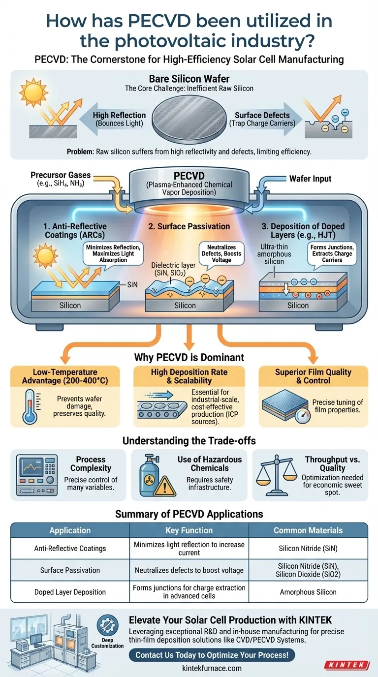
In the photovoltaic industry, PECVD is a cornerstone technology used to deposit critical thin films onto crystalline silicon solar cells. These films serve as anti-reflective coatings to maximize light absorption and as passivation layers to neutralize electrical defects on the silicon surface. The primary goal of using Plasma-Enhanced Chemical Vapor Deposition (PECVD) is to significantly enhance the overall efficiency and long-term durability of the finished solar panel.
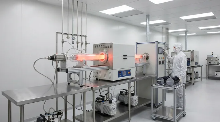
The core challenge in solar cell manufacturing is adding high-performance functional layers without damaging the underlying silicon wafer. PECVD is the dominant solution because its low-temperature plasma process allows for the high-speed deposition of superior-quality films, making it perfectly suited for cost-effective, industrial-scale production.
The Core Challenge: Maximizing Solar Cell Efficiency
Why Raw Silicon Isn't Enough
A bare, polished silicon wafer is not an efficient solar cell on its own. It suffers from two fundamental loss mechanisms: high surface reflectivity, which bounces valuable sunlight away, and surface defects, which trap the electrical charge carriers (electrons and holes) generated by light.
The Role of Functional Thin Films
To overcome these limitations, manufacturers add several ultra-thin layers to the wafer's surface. Each layer performs a specific function, and their combined effect is what transforms a simple silicon wafer into a high-efficiency photovoltaic device. This is where PECVD becomes indispensable.
PECVD's Critical Roles in Solar Cell Fabrication
Anti-Reflective Coatings (ARCs)
The most visible application of PECVD is the creation of an anti-reflective coating, which gives modern solar cells their characteristic deep blue or black appearance.
This layer, typically made of silicon nitride (SiN), is precisely engineered to a specific thickness to minimize light reflection from the cell's surface. By ensuring more photons enter the silicon, the ARC directly increases the amount of current the cell can generate.
Surface Passivation
Surface passivation is an invisible but arguably more critical function for boosting cell efficiency. The surfaces and edges of a silicon wafer are full of atomic-level imperfections that act as "traps" for charge carriers.
PECVD is used to deposit a dielectric layer, such as silicon nitride (SiN) or silicon dioxide (SiO2), that effectively neutralizes these defects. This "passivation" prevents electrons and holes from being lost, which dramatically increases the cell's voltage and overall power output. Often, the silicon nitride ARC serves the dual purpose of both anti-reflection and surface passivation.
Deposition of Doped Layers
In more advanced solar cell architectures, such as HJT (Heterojunction with Intrinsic Thin layer), PECVD is also used to deposit ultra-thin layers of amorphous (non-crystalline) silicon. These layers form critical semiconductor junctions that are exceptionally effective at separating and extracting charge carriers.
Why PECVD is the Dominant Technology
The Low-Temperature Advantage
The most significant benefit of PECVD is its ability to operate at low temperatures (typically 200-400°C). Alternative methods like thermal chemical vapor deposition require much higher temperatures that can degrade the sensitive properties of the high-quality silicon wafer, negating its performance potential.
High Deposition Rate for Scalability
For solar to be cost-effective, manufacturing must be fast and scalable. Modern PECVD systems, often using Inductively Coupled Plasma (ICP) sources, enable "high-rate inline deposition." This allows for the rapid, continuous processing of wafers, which is essential for mass production and lowering the cost-per-watt.
Superior Film Quality and Control
The plasma environment in a PECVD reactor provides a high density of reactive species at low ion energy. This allows for the formation of extremely dense, uniform, and high-quality films. This process control is vital for tuning a film's properties, such as the precise refractive index of an ARC or the defect-passivating ability of a dielectric layer.
Understanding the Trade-offs
Process Complexity
PECVD systems are sophisticated machines that require precise control over numerous variables, including gas mixtures, pressure, plasma power, and temperature. Maintaining process stability and uniformity across millions of wafers is a significant engineering challenge.
Use of Precursor Chemicals
The process relies on precursor gases, such as silane (SiH₄) and ammonia (NH₃), which can be hazardous. Operating a PECVD facility requires substantial investment in safety protocols, gas handling infrastructure, and abatement systems.
Throughput vs. Quality
While PECVD enables high throughput, there is an inherent trade-off between deposition speed and ultimate film quality. Manufacturers must constantly optimize their processes to find the economic sweet spot that delivers high-performance cells at a competitive cost.
Making the Right Choice for Your Goal
- If your primary focus is increasing cell efficiency: Master the PECVD process to deposit the highest quality passivation and anti-reflective layers, as these directly boost the cell's voltage and current.
- If your primary focus is manufacturing and cost reduction: Leverage the high-throughput capabilities of modern inline PECVD tools to lower the cycle time and reduce the manufacturing cost-per-watt.
- If your primary focus is research and development: Utilize the flexibility of PECVD to experiment with novel materials and deposit the complex, multi-layer stacks required for next-generation cell architectures.
Understanding PECVD's function is fundamental to understanding how modern, high-efficiency solar cells are made both possible and affordable.
Summary Table:
| Application | Key Function | Common Materials |
|---|---|---|
| Anti-Reflective Coatings | Minimizes light reflection to increase current | Silicon Nitride (SiN) |
| Surface Passivation | Neutralizes defects to boost voltage | Silicon Nitride (SiN), Silicon Dioxide (SiO2) |
| Doped Layer Deposition | Forms junctions for charge extraction in advanced cells | Amorphous Silicon |
Elevate your solar cell production with KINTEK's advanced PECVD solutions! Leveraging exceptional R&D and in-house manufacturing, we provide diverse laboratories with high-temperature furnace systems like CVD/PECVD Systems, designed for precise thin-film deposition. Our strong deep customization capability ensures tailored solutions to meet your unique experimental needs, enhancing efficiency and scalability. Contact us today to discuss how we can optimize your photovoltaic processes!
Visual Guide
Related Products
- Slide PECVD Tube Furnace with Liquid Gasifier PECVD Machine
- RF PECVD System Radio Frequency Plasma Enhanced Chemical Vapor Deposition
- Inclined Rotary Plasma Enhanced Chemical Deposition PECVD Tube Furnace Machine
- Inclined Rotary Plasma Enhanced Chemical Deposition PECVD Tube Furnace Machine
- Multi Heating Zones CVD Tube Furnace Machine for Chemical Vapor Deposition Equipment
People Also Ask
- What are the main advantages of PECVD tube furnaces compared to CVD tube furnaces? Lower Temp, Faster Deposition, and More
- How does a hydrogen reduction environment in an industrial tube furnace facilitate gold-copper alloy microspheres?
- What are the disadvantages of tube furnace cracking when processing heavy raw materials? Avoid Costly Downtime and Inefficiency
- How does PECVD equipment contribute to TOPCon bottom cells? Mastering Hydrogenation for Maximum Solar Efficiency
- What are the typical conditions for plasma-enhanced CVD processes? Achieve Low-Temperature Thin Film Deposition


