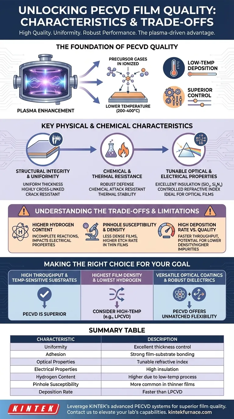
At its core, films produced by Plasma-Enhanced Chemical Vapor Deposition (PECVD) are characterized by their high quality, uniformity, and robust performance across a range of applications. The plasma-driven process enables the growth of films with excellent adhesion, resistance to cracking, and precisely controlled optical and electrical properties, all while operating at significantly lower temperatures than conventional CVD methods.
PECVD's defining advantage is its ability to produce versatile, high-quality films on temperature-sensitive materials. However, this low-temperature benefit introduces a critical trade-off: the films often contain higher hydrogen content and can be more susceptible to pinholes than those grown at higher temperatures.
The Foundation of PECVD Film Quality
The unique characteristics of PECVD films stem directly from its use of plasma to energize precursor gases. This fundamental difference from thermally-driven processes like Low-Pressure CVD (LPCVD) dictates the final properties of the film.
The Role of Plasma Enhancement
In a PECVD system, an electrical field creates a plasma, which is a high-energy state of ionized gas. This plasma effectively breaks down the precursor gas molecules into highly reactive species.
This increased reactivity allows deposition to occur at much lower substrate temperatures (e.g., 200-400°C) compared to the high temperatures (600-800°C+) required for traditional CVD.
Superior Control Over Film Properties
The plasma process gives operators exceptional control over the final film. By precisely adjusting parameters like gas flow rates, plasma power, pressure, and temperature, you can directly manipulate the film's final characteristics.
This allows for fine-tuning of properties such as internal stress, refractive index, and hardness to meet specific device requirements.
Excellent Conformality and Coverage
PECVD provides good three-dimensional coverage over complex surface topographies. This makes it more effective than line-of-sight deposition techniques, such as Physical Vapor Deposition (PVD), for coating intricate structures found in modern microelectronics.
Key Physical and Chemical Characteristics
PECVD films are valued for a consistent set of desirable physical, chemical, and functional properties.
Structural Integrity and Uniformity
Films deposited via PECVD are known for their uniform thickness across the entire substrate. They are also highly cross-linked, which contributes to their structural integrity and strong resistance to cracking.
Chemical and Thermal Resistance
The dense, cross-linked nature of these films makes them highly robust. They exhibit outstanding resistance to chemical attack and can withstand significant thermal changes without degrading, making them suitable for protective coatings.
Tunable Optical and Electrical Properties
PECVD is a dominant technology for fabricating optical and dielectric layers. Materials like silicon oxide (SiO₂) and silicon nitride (Si₃N₄) can be deposited with excellent electrical insulation.
Furthermore, the ability to control the refractive index makes PECVD ideal for creating anti-reflective coatings and other optical films.
Understanding the Trade-offs and Limitations
No deposition technique is perfect. The low-temperature nature of PECVD, while a primary benefit, also introduces specific compromises that are critical to understand.
The Issue of Hydrogen Content
Because the precursor gases (e.g., silane, SiH₄) are broken down by plasma energy rather than extreme heat, the chemical reactions are not always complete. This often results in hydrogen atoms from the precursors being incorporated into the deposited film.
This elevated hydrogen content can impact the film's electrical properties and long-term stability, a factor that must be managed for sensitive electronic applications.
Pinholes and Film Density
Films deposited at lower temperatures tend to be less dense than their high-temperature counterparts. This can lead to a higher susceptibility to pinholes, which are microscopic defects that can compromise a film's barrier properties.
This effect is particularly notable in thinner films (under ~4000 Å) and can result in a higher etch rate compared to denser films from processes like LPCVD.
High Deposition Rate vs. Film Quality
PECVD offers significantly higher deposition rates than many other methods, which is a major advantage for manufacturing throughput. For example, PECVD silicon nitride can be deposited orders of magnitude faster than with LPCVD.
However, this speed can sometimes come at the expense of achieving the absolute highest film density and lowest impurity levels possible with slower, higher-temperature processes.
Making the Right Choice for Your Goal
Selecting a deposition method requires balancing the needs of your substrate, your performance targets, and your manufacturing goals.
- If your primary focus is high throughput and processing on temperature-sensitive substrates (like polymers or pre-processed wafers): PECVD is the superior choice due to its low thermal budget and high deposition rates.
- If your primary focus is achieving the absolute highest film density and lowest hydrogen content for a critical electronic layer: A high-temperature process like LPCVD may be more suitable, assuming your substrate can withstand the heat.
- If your primary focus is creating versatile optical coatings or robust dielectric layers: PECVD offers an unmatched combination of property control, efficiency, and material flexibility.
By understanding this balance between low-temperature flexibility and film composition, you can effectively leverage PECVD to achieve a vast range of advanced material and device goals.
Summary Table:
| Characteristic | Description |
|---|---|
| Uniformity | Excellent thickness control across substrates |
| Adhesion | Strong film-substrate bonding |
| Optical Properties | Tunable refractive index for coatings |
| Electrical Properties | High insulation for dielectric layers |
| Hydrogen Content | Higher due to low-temperature process |
| Pinhole Susceptibility | More common in thinner films |
| Deposition Rate | Faster than LPCVD, aiding throughput |
Leverage KINTEK's exceptional R&D and in-house manufacturing to elevate your lab's capabilities with advanced PECVD systems. Our high-temperature furnace solutions, including CVD/PECVD Systems, are tailored for diverse laboratories, offering deep customization to meet your unique experimental needs. Achieve superior film quality with precise control—contact us today to discuss how we can enhance your research and production processes!
Visual Guide
Related Products
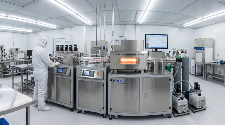
- RF PECVD System Radio Frequency Plasma Enhanced Chemical Vapor Deposition
- Slide PECVD Tube Furnace with Liquid Gasifier PECVD Machine
- Inclined Rotary Plasma Enhanced Chemical Deposition PECVD Tube Furnace Machine
- Inclined Rotary Plasma Enhanced Chemical Deposition PECVD Tube Furnace Machine
People Also Ask
- What is the role of RF power in PECVD and how does the RF-PECVD process work? Master Thin Film Deposition Control
- How is silicon dioxide deposited from tetraethylorthosilicate (TEOS) in PECVD? Achieve Low-Temperature, High-Quality SiO2 Films
- What are the applications of plasma enhanced chemical vapor deposition? Key Uses in Electronics, Optics & Materials
- What are the key advantages of PECVD technology? Achieve Low-Temperature, High-Quality Thin Film Deposition
- How are deposition rates and film properties controlled in PECVD? Master Key Parameters for Optimal Thin Films


