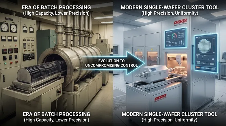
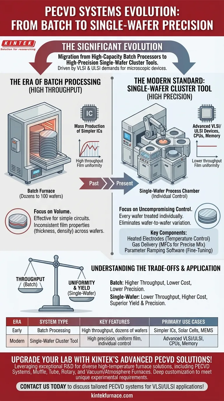
The most significant evolution in PECVD systems was the migration from high-capacity batch processors to high-precision single-wafer cluster tools. This fundamental shift was not merely a change in machinery but a direct response to the demands of modern electronics. The advent of Very Large Scale Integration (VLSI) and Ultra Large Scale Integration (ULSI) circuits, where device features shrank to microscopic levels, made the wafer-to-wafer variations of older batch systems unacceptable.
The evolution from batch to single-wafer PECVD was driven by one non-negotiable requirement: the need for absolute process control. As semiconductor devices became smaller and more complex, the industry traded the raw throughput of batch systems for the uncompromising uniformity and precision of single-wafer processing.
The Driving Force: From High Throughput to High Precision
The story of PECVD's evolution is the story of the semiconductor industry itself. The core goal has always been to deposit thin films, but the definition of a "good" film has changed dramatically.
The Era of Batch Processing
In earlier generations of manufacturing, efficiency was measured by volume. Batch processors were large furnaces that could handle dozens or even up to 100 wafers in a single run.
This approach was effective for its time, enabling the mass production of simpler integrated circuits. However, it was nearly impossible to ensure every wafer in the batch experienced the exact same conditions, leading to slight variations in film properties.
The VLSI/ULSI Revolution
The development of VLSI and ULSI technologies marked a critical turning point. As transistors and other components shrank, even minuscule inconsistencies in film thickness, density, or chemical composition could ruin a device.
The industry needed a system where the process for wafer #1 was identical to the process for wafer #1000. The variability of batch processing became a critical liability, demanding a new approach.
The Modern Standard: The Single-Wafer Cluster Tool
To solve the uniformity crisis, the industry developed the single-wafer cluster tool. This architecture abandoned the batch concept in favor of treating each wafer as an individual, isolated process.
A Focus on Uncompromising Control
In a modern system, a single wafer enters a dedicated PECVD process chamber. Here, it is subjected to a precisely controlled environment, ensuring the resulting film is perfectly uniform across its entire surface.
This one-at-a-time approach guarantees that every wafer produced receives the exact same treatment, eliminating the primary weakness of the older batch systems.
Key Components for Precision Deposition
Modern PECVD systems achieve this control through highly engineered subsystems:
- Heated Electrodes: An upper and lower electrode create the plasma and precisely control the substrate temperature, a critical factor for film quality.
- Gas Delivery: A multi-line gas pod with mass-flow controllers (MFCs) delivers an exact, repeatable mixture of precursor gases into the chamber.
- Parameter Ramping Software: Sophisticated software allows operators to finely tune and ramp process parameters—like temperature, pressure, and gas flow—during the deposition itself.
The Power of Fine-Tuning
This level of control allows for the deliberate manipulation of key film properties. By adjusting gas flow rates, operating temperature, and plasma conditions, engineers can precisely determine the film's final thickness, refractive index, internal stress, and hardness.
Understanding the Trade-offs
The transition to single-wafer systems was not without its compromises. Understanding these trade-offs is key to appreciating why the shift was necessary.
Throughput vs. Uniformity
The most obvious trade-off is raw wafer throughput. A batch furnace could process 100 wafers simultaneously. While modern single-wafer chambers are very fast, the overall system throughput is inherently lower.
However, this is a misleading comparison. The "yield"—the percentage of usable, functioning chips—from a single-wafer system is vastly higher for advanced devices, making its effective throughput superior.
Cost and Complexity
Single-wafer cluster tools are significantly more complex and expensive than their batch predecessors. They require advanced vacuum technology, sophisticated control electronics, and robotics to move wafers between process modules.
This higher cost is the necessary price for the precision required to manufacture modern CPUs, memory chips, and other advanced processors.
How to Apply This to Your Goal
The choice between these technological generations is dictated entirely by the sensitivity of the device being manufactured.
- If your primary focus is leading-edge process control and film uniformity: The single-wafer cluster tool is the only viable option for manufacturing advanced VLSI/ULSI devices.
- If your primary focus is high-volume deposition for less sensitive applications: Older batch systems may still find use in areas like solar cell or some MEMS manufacturing, where cost-per-wafer is more critical than nanometer-level uniformity.
Ultimately, the evolution of PECVD technology mirrors the relentless pursuit of precision that defines the entire semiconductor industry.
Summary Table:
| Era | System Type | Key Features | Primary Use Cases |
|---|---|---|---|
| Early | Batch Processing | High throughput, handles dozens of wafers | Mass production of simpler ICs, solar cells, some MEMS |
| Modern | Single-Wafer Cluster Tool | High precision, uniform film deposition, individual wafer control | Advanced VLSI/ULSI devices, CPUs, memory chips |
Upgrade Your Lab with KINTEK's Advanced PECVD Solutions!
Are you working on cutting-edge semiconductor research or manufacturing that demands absolute process control and film uniformity? KINTEK leverages exceptional R&D and in-house manufacturing to provide diverse laboratories with advanced high-temperature furnace solutions. Our product line includes PECVD Systems, Muffle, Tube, Rotary Furnaces, and Vacuum & Atmosphere Furnaces, complemented by strong deep customization capabilities to precisely meet your unique experimental requirements.
Contact us today to discuss how our tailored PECVD systems can enhance your precision and yield in VLSI/ULSI applications!
Visual Guide
Related Products
- RF PECVD System Radio Frequency Plasma Enhanced Chemical Vapor Deposition
- Slide PECVD Tube Furnace with Liquid Gasifier PECVD Machine
- Inclined Rotary Plasma Enhanced Chemical Deposition PECVD Tube Furnace Machine
- Inclined Rotary Plasma Enhanced Chemical Deposition PECVD Tube Furnace Machine
- Cylindrical Resonator MPCVD Machine System for Lab Diamond Growth
People Also Ask
- How are deposition rates and film properties controlled in PECVD? Master Key Parameters for Optimal Thin Films
- What are some promising applications of PECVD-prepared 2D materials? Unlock Advanced Sensing and Optoelectronics
- How is silicon dioxide deposited from tetraethylorthosilicate (TEOS) in PECVD? Achieve Low-Temperature, High-Quality SiO2 Films
- What are the advantages of PECVD in film deposition? Achieve Low-Temp, High-Quality Coatings
- What are the applications of plasma enhanced chemical vapor deposition? Key Uses in Electronics, Optics & Materials


