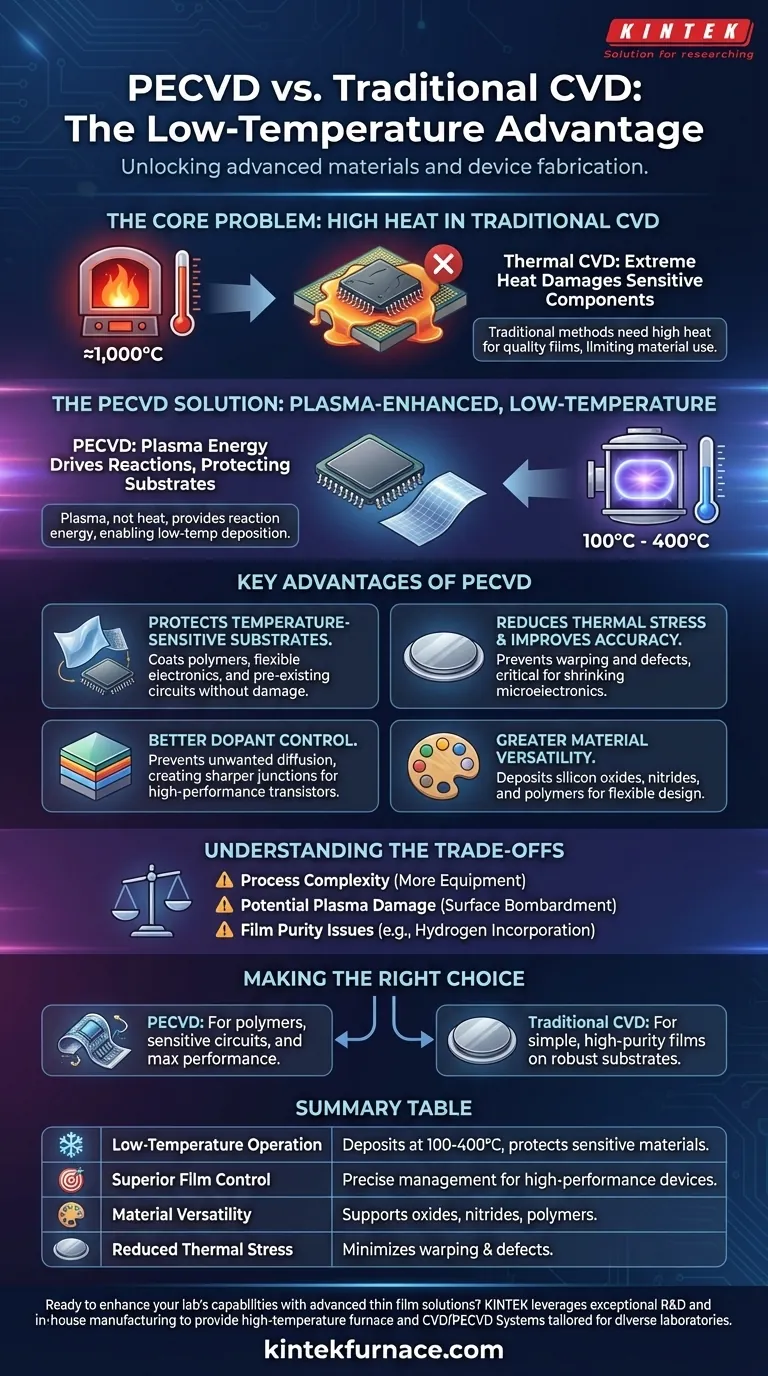
The fundamental advantage of PECVD is its ability to deposit high-quality thin films at significantly lower temperatures than traditional Chemical Vapor Deposition (CVD) methods. By using plasma instead of high heat to drive chemical reactions, PECVD avoids damaging heat-sensitive components, enabling the creation of modern, complex electronic devices. This low-temperature operation also provides superior control over film properties and broadens the range of materials that can be deposited.
Traditional deposition methods are limited by a simple rule: high heat is required to create high-quality films. PECVD breaks this rule by using energized plasma to do the work of heat, unlocking the ability to coat sensitive, modern materials without destroying them.
The Core Problem: High Heat in Traditional CVD
How Thermal CVD Works
Traditional thermal CVD relies exclusively on very high temperatures, often around 1,000°C, to give precursor gas molecules enough energy to react and form a solid film on a substrate.
This process is effective but acts like a furnace, subjecting everything inside to extreme thermal stress.
The Limitation of Heat
This high-heat requirement makes thermal CVD incompatible with many modern manufacturing needs. Substrates like polymers (plastics) or devices with pre-existing, delicate electronic circuits would be damaged or destroyed at these temperatures.
How PECVD Solves the Temperature Challenge
Using Plasma Instead of Heat
Plasma-Enhanced Chemical Vapor Deposition (PECVD) operates on a different principle. It takes place inside a vacuum chamber where an electric field is used to ionize a gas, creating plasma.
This plasma—a highly energized state of matter—provides the energy needed to break apart precursor gases and initiate the chemical reactions for film deposition.
The Impact of Plasma-Energized Reactions
Because the plasma, not heat, is doing the heavy lifting, the substrate itself can remain at a much lower temperature, typically between 100°C and 400°C.
This dramatic reduction in temperature is the primary reason PECVD is a cornerstone of modern fabrication.
Key Advantages Stemming from Low-Temperature Operation
Protecting Temperature-Sensitive Substrates
The most significant advantage is the ability to coat materials that cannot withstand high heat. This includes flexible plastics, polymers, and complex silicon wafers that already contain intricate, low-melting-point metallic circuitry.
Reducing Thermal Stress and Improving Accuracy
Even on substrates that can tolerate heat, the lower temperature of PECVD reduces thermal stress. This prevents warping and the formation of defects, which is critical as the dimensions of microelectronic devices continue to shrink.
Better Dopant Control
In semiconductor manufacturing, lower temperatures prevent the unwanted diffusion of dopants already present in the microchip. This allows for the creation of sharper, more defined junctions, which is essential for high-performance transistors.
Greater Material Versatility
PECVD can be used to deposit a much wider range of materials than many other methods, including silicon oxides, nitrides, and even polymers. This gives engineers immense flexibility in material and device design.
Understanding the Trade-offs
Process Complexity
The use of plasma requires more complex and expensive equipment than a simple thermal CVD furnace. This includes RF power generators, vacuum systems, and sophisticated controls to manage the plasma environment.
Potential for Plasma Damage
While plasma enables low-temperature processing, the high-energy ions can physically bombard the substrate surface. If not carefully controlled, this can cause structural damage or introduce defects into the film or the underlying device.
Film Purity
The complex chemical reactions within the plasma can sometimes lead to the incorporation of unintended elements, like hydrogen, into the deposited film. This can affect the film's electrical and mechanical properties and must be carefully managed.
Making the Right Choice for Your Goal
Choosing a deposition method depends entirely on the requirements of your substrate and the desired properties of the final film.
- If your primary focus is working with polymers, flexible substrates, or completed circuits: PECVD is the necessary choice to prevent thermal damage.
- If your primary focus is depositing a simple, high-purity film on a robust substrate like a bare silicon wafer: Traditional thermal CVD can be a simpler and effective option.
- If your primary focus is maximum performance and design flexibility for advanced devices: PECVD offers superior control over film properties and a wider palette of materials.
Ultimately, PECVD's ability to decouple the reaction energy from thermal energy is what makes it an indispensable tool for fabricating the next generation of technology.
Summary Table:
| Advantage | Description |
|---|---|
| Low-Temperature Operation | Deposits films at 100-400°C, protecting heat-sensitive materials like polymers and circuits. |
| Superior Film Control | Enables precise management of film properties and dopants for high-performance devices. |
| Material Versatility | Supports deposition of silicon oxides, nitrides, and polymers, expanding design options. |
| Reduced Thermal Stress | Minimizes warping and defects in substrates, crucial for shrinking microelectronics. |
Ready to enhance your lab's capabilities with advanced thin film solutions? At KINTEK, we leverage exceptional R&D and in-house manufacturing to provide high-temperature furnace solutions tailored for diverse laboratories. Our product line includes Muffle, Tube, Rotary Furnaces, Vacuum & Atmosphere Furnaces, and CVD/PECVD Systems, all backed by strong deep customization to meet your unique experimental needs. Contact us today to discuss how our PECVD systems can drive innovation in your projects!
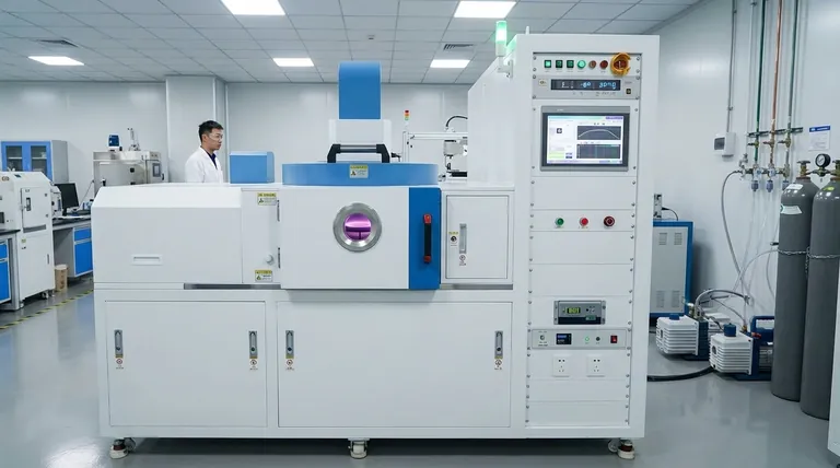
Visual Guide
Related Products
- Slide PECVD Tube Furnace with Liquid Gasifier PECVD Machine
- RF PECVD System Radio Frequency Plasma Enhanced Chemical Vapor Deposition
- Inclined Rotary Plasma Enhanced Chemical Deposition PECVD Tube Furnace Machine
- Inclined Rotary Plasma Enhanced Chemical Deposition PECVD Tube Furnace Machine
- Multi Heating Zones CVD Tube Furnace Machine for Chemical Vapor Deposition Equipment
People Also Ask
- What role does a Tube Furnace play in the CVD growth of carbon nanotubes? Achieve High-Purity CNT Synthesis
- What is plasma in the context of PECVD? Unlock Low-Temperature Thin Film Deposition
- How does a hydrogen reduction environment in an industrial tube furnace facilitate gold-copper alloy microspheres?
- What plasma source is used in PE-CVD tube furnaces? Unlock Low-Temperature, High-Quality Deposition
- How does PECVD equipment contribute to TOPCon bottom cells? Mastering Hydrogenation for Maximum Solar Efficiency


