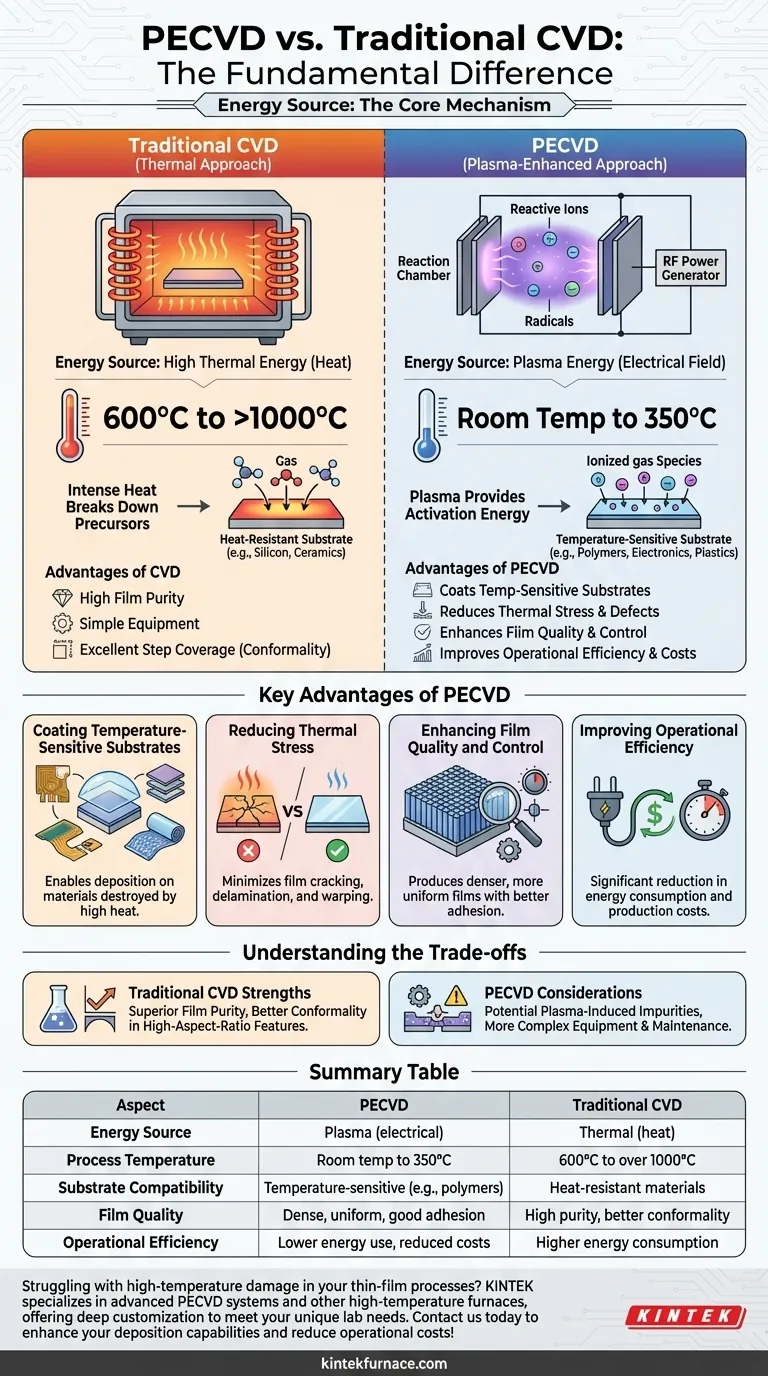
The fundamental difference between Plasma-Enhanced Chemical Vapor Deposition (PECVD) and conventional Chemical Vapor Deposition (CVD) is the energy source used to drive the reaction. While traditional CVD relies exclusively on high thermal energy (heat) to break down precursor gases, PECVD utilizes an energy-efficient plasma to achieve the same result at significantly lower temperatures. This allows PECVD to deposit high-quality films on materials that would be damaged or destroyed by the intense heat of a conventional CVD process.
The choice between PECVD and conventional CVD is a choice between energy sources. Traditional CVD uses thermal energy, requiring high heat. PECVD uses plasma energy, enabling low-temperature deposition. This single difference dictates which substrates you can use, the final film quality, and your operational costs.
The Core Mechanism: Thermal vs. Plasma Energy
To understand the practical differences, you must first understand how each process supplies the energy needed to create a thin film from a gas.
Traditional CVD: The Thermal Approach
Conventional CVD is conceptually straightforward. Precursor gases are introduced into a reaction chamber containing a heated substrate.
The intense heat, typically ranging from 600°C to over 1000°C, provides the thermal energy required to trigger chemical reactions. These reactions break the gases down into their atomic components, which then deposit onto the hot substrate, gradually building a solid film.
PECVD: The Plasma-Enhanced Approach
PECVD replaces most of the required thermal energy with electrical energy. An electric field is applied to the precursor gas, creating a plasma—an ionized gas containing highly reactive ions and free radicals.
These reactive species are far more chemically volatile than the original gas molecules. They readily react and deposit onto the substrate even at low temperatures, typically between room temperature and 350°C. The plasma provides the activation energy, not the heat.
Key Advantages of the PECVD Process
The use of plasma instead of high heat gives PECVD several distinct advantages that make it essential for modern manufacturing, particularly in semiconductors and electronics.
Coating Temperature-Sensitive Substrates
This is the most significant advantage of PECVD. The low process temperature allows for the deposition of films on materials that cannot withstand high heat.
This includes substrates like polymers, plastics, and certain metals or assembled electronic components. A traditional CVD process would simply melt, warp, or destroy them.
Reducing Thermal Stress
Even for substrates that can withstand high heat, the extreme temperatures of conventional CVD can induce significant thermal stress. This leads to film cracking, delamination, or warping of the substrate.
PECVD’s low-temperature environment minimizes this stress, resulting in more durable and reliable films with a lower defect density.
Enhancing Film Quality and Control
The energy from the plasma allows for a high deposition rate while maintaining excellent control over the film's properties.
PECVD can produce films that are denser, more uniform, and have better adhesion than those from some low-temperature CVD alternatives. The plasma parameters can be tuned to precisely control film characteristics like stoichiometry and stress.
Improving Operational Efficiency
By eliminating the need for extreme heating, PECVD significantly reduces energy consumption and production costs.
Chamber cleaning can also be easier and faster, as the lower temperatures often result in less baked-on residue compared to high-temperature reactors, improving overall equipment uptime and throughput.
Understanding the Trade-offs
While PECVD is incredibly versatile, conventional CVD is not obsolete. It remains the superior choice for specific applications where its unique characteristics are required.
Film Purity and Composition
The plasma in a PECVD process can sometimes lead to the incorporation of other elements (like hydrogen from precursor gases) into the film. For applications demanding the absolute highest material purity, the cleaner, thermally-driven reaction of conventional CVD may be preferable, provided the substrate can tolerate the heat.
Equipment Simplicity
A traditional thermal CVD reactor is, at its core, a high-temperature furnace with gas flow control. A PECVD system is more complex, requiring RF power generators, impedance matching networks, and more sophisticated vacuum technology to generate and sustain the plasma. This can translate to higher initial equipment costs and maintenance complexity.
Step Coverage in High-Aspect-Ratio Features
For depositing films inside very deep and narrow trenches (high-aspect-ratio structures), high-temperature CVD can sometimes provide better conformality, or step coverage. The high thermal energy gives deposited atoms more surface mobility, allowing them to migrate and evenly coat complex topographies more effectively than the more directional deposition typical of some PECVD processes.
Making the Right Choice for Your Application
Selecting the correct deposition method requires matching the process capabilities to your specific technical and economic goals.
- If your primary focus is coating temperature-sensitive materials: PECVD is the only viable choice. Its low-temperature nature is its defining advantage.
- If your primary focus is the highest possible film purity on a robust substrate: Conventional CVD should be evaluated, as it avoids potential plasma-induced contamination.
- If your primary focus is reducing operational cost and energy use for high-volume production: PECVD is generally the more efficient and cost-effective solution.
- If your primary focus is achieving perfect conformality in deep trenches: High-temperature conventional CVD often holds an advantage due to enhanced surface atom mobility.
Ultimately, your decision hinges on the thermal budget of your substrate and the specific film properties your application demands.
Summary Table:
| Aspect | PECVD | Traditional CVD |
|---|---|---|
| Energy Source | Plasma (electrical) | Thermal (heat) |
| Process Temperature | Room temp to 350°C | 600°C to over 1000°C |
| Substrate Compatibility | Temperature-sensitive (e.g., polymers, electronics) | Heat-resistant materials |
| Film Quality | Dense, uniform, good adhesion | High purity, better conformality |
| Operational Efficiency | Lower energy use, reduced costs | Higher energy consumption |
Struggling with high-temperature damage in your thin-film processes? KINTEK specializes in advanced PECVD systems and other high-temperature furnaces, offering deep customization to meet your unique lab needs. Our expertise in R&D and in-house manufacturing ensures reliable, efficient solutions for temperature-sensitive applications. Contact us today to enhance your deposition capabilities and reduce operational costs!
Visual Guide
Related Products
- RF PECVD System Radio Frequency Plasma Enhanced Chemical Vapor Deposition
- Slide PECVD Tube Furnace with Liquid Gasifier PECVD Machine
- Inclined Rotary Plasma Enhanced Chemical Deposition PECVD Tube Furnace Machine
- Inclined Rotary Plasma Enhanced Chemical Deposition PECVD Tube Furnace Machine
- Cylindrical Resonator MPCVD Machine System for Lab Diamond Growth
People Also Ask
- What are some promising applications of PECVD-prepared 2D materials? Unlock Advanced Sensing and Optoelectronics
- What is the role of RF power in PECVD and how does the RF-PECVD process work? Master Thin Film Deposition Control
- What is PECVD specification? A Guide to Choosing the Right System for Your Lab
- How does film quality compare between PECVD and CVD? Choose the Best Method for Your Substrate
- How is silicon dioxide deposited from tetraethylorthosilicate (TEOS) in PECVD? Achieve Low-Temperature, High-Quality SiO2 Films


