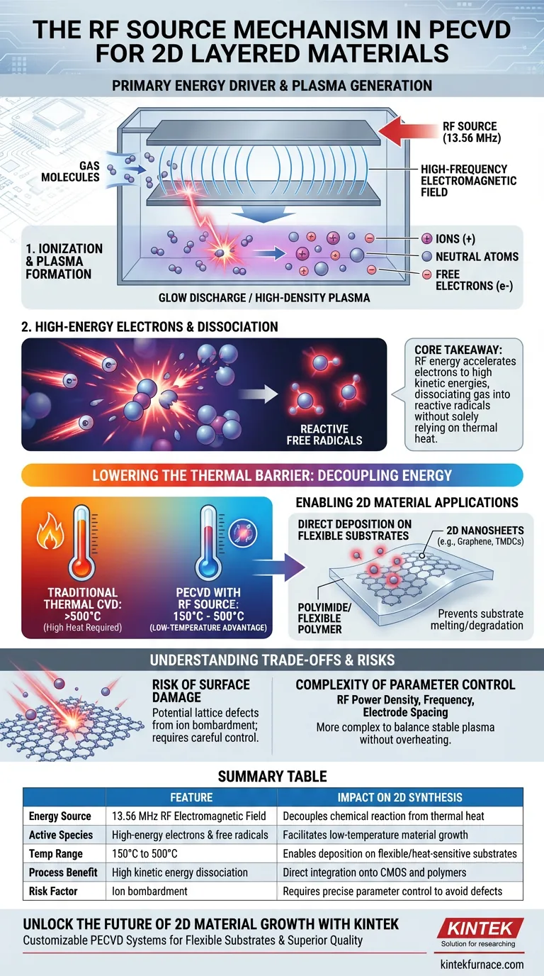
The radio frequency (RF) source acts as the primary energy driver in the PECVD process. It generates a high-frequency electromagnetic field—typically at 13.56 MHz—that ionizes process gases into a high-density plasma. This ionization creates high-energy electrons that collide with gas molecules, dissociating them into reactive free radicals required for material deposition.
Core Takeaway By utilizing RF energy to accelerate electrons rather than relying solely on thermal heat, PECVD decouples the chemical reaction energy from the substrate temperature. This allows high-quality 2D materials to be synthesized at significantly lower temperatures (150°C–500°C), enabling direct deposition onto heat-sensitive, flexible substrates.
The Mechanics of Plasma Generation
Creating the Electromagnetic Field
The process begins when the RF source applies a high-frequency oscillating voltage between two electrodes.
This creates a dynamic electromagnetic field within the reaction chamber, which serves as the power source for the gas decomposition.
Ionization and Plasma Formation
As the process gases flow through this field, the electromagnetic energy strips electrons from the gas atoms.
This ionization event transforms the neutral gas into a "glow discharge" or high-density plasma, consisting of ions, neutral atoms, and free electrons.
The Role of High-Energy Electrons
Within this plasma, the free electrons are accelerated by the RF field to extremely high kinetic energies.
These high-energy electrons collide violently with the remaining neutral gas molecules.
Dissociation into Free Radicals
The collisions transfer energy to the gas molecules, causing them to break apart (dissociate).
This results in the formation of active free radicals—highly reactive chemical species that are the fundamental building blocks for the 2D material layers.
Lowering the Thermal Barrier
Replacing Thermal Energy with Kinetic Energy
In traditional thermal CVD, the substrate must be heated to very high temperatures to provide the energy needed to break chemical bonds.
In PECVD, the RF source supplies this energy via electron impact. The gas is "hot" (chemically reactive) while the ions and neutral species remain relatively "cool."
The 150°C to 500°C Advantage
Because the reaction is initiated by plasma energy, the substrate does not need to drive the reaction thermally.
This allows the deposition process to occur at temperatures between 150°C and 500°C, which is significantly lower than the requirements for standard thermal CVD.
Enabling 2D Material Applications
Direct Deposition on Flexible Substrates
The reduced temperature requirement is the critical factor for synthesizing two-dimensional layered materials on non-traditional surfaces.
It becomes possible to deposit nanosheets directly onto flexible polymers like polyimide, which would melt or degrade under thermal CVD conditions.
Synthesizing Nanosheets
The active free radicals generated by the RF source adsorb onto the substrate surface.
They react and bond to form continuous, two-dimensional crystalline structures, such as graphene or transition metal dichalcogenides (TMDCs).
Understanding the Trade-offs
Risk of Surface Damage
While the RF source provides necessary energy, the plasma also contains high-energy ions.
If not carefully controlled, these ions can bombard the growing 2D lattice, potentially creating defects or degrading the crystalline quality of delicate nanosheets.
Complexity of Parameter Control
The introduction of an RF source adds variables such as power density, frequency, and electrode spacing to the process window.
Balancing these factors to maintain a stable plasma without overheating the substrate requires more complex process control than simple thermal systems.
Making the Right Choice for Your Goal
- If your primary focus is flexible electronics: The RF source is essential; it allows you to utilize polymer substrates (like polyimide) by keeping process temperatures below their glass transition points.
- If your primary focus is low-temperature integration: Use the RF mechanism to deposit 2D materials directly onto finished circuits (CMOS back-end) without damaging existing thermal-sensitive components.
The RF source effectively transforms the PECVD chamber into a high-energy chemical reactor that respects the thermal limits of your substrate.
Summary Table:
| Feature | Description | Impact on 2D Synthesis |
|---|---|---|
| Energy Source | 13.56 MHz RF Electromagnetic Field | Decouples chemical reaction from thermal heat |
| Active Species | High-energy electrons & free radicals | Facilitates low-temperature material growth |
| Temp Range | 150°C to 500°C | Enables deposition on flexible/heat-sensitive substrates |
| Process Benefit | High kinetic energy dissociation | Direct integration onto CMOS and polymers |
| Risk Factor | Ion bombardment | Requires precise parameter control to avoid lattice defects |
Unlock the Future of 2D Material Growth with KINTEK
Are you looking to revolutionize your electronics with low-temperature graphene or TMDC synthesis? Backed by expert R&D and world-class manufacturing, KINTEK offers high-performance CVD and PECVD systems—including specialized Muffle, Tube, Rotary, and Vacuum furnaces—all customizable for your unique lab requirements.
Our advanced RF-powered solutions allow you to achieve precise deposition on flexible substrates while maintaining superior crystalline quality. Contact us today to discuss your specific high-temperature lab needs and discover how our custom-engineered systems can accelerate your research and production goals.
Visual Guide
References
- O. Ozturk, Emre Gür. Layered Transition Metal Sulfides for Supercapacitor Applications. DOI: 10.1002/celc.202300575
This article is also based on technical information from Kintek Furnace Knowledge Base .
Related Products
- Slide PECVD Tube Furnace with Liquid Gasifier PECVD Machine
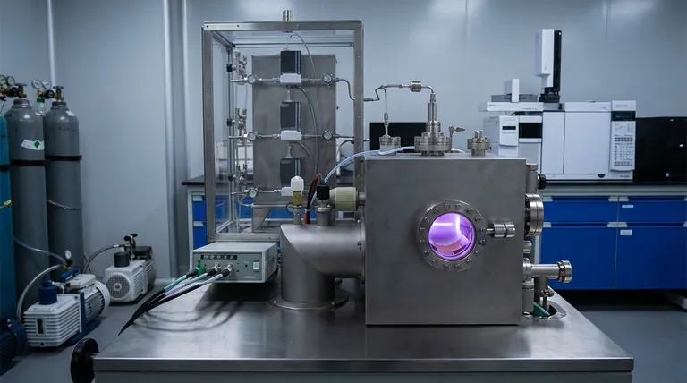
- RF PECVD System Radio Frequency Plasma Enhanced Chemical Vapor Deposition
- Inclined Rotary Plasma Enhanced Chemical Deposition PECVD Tube Furnace Machine
- Inclined Rotary Plasma Enhanced Chemical Deposition PECVD Tube Furnace Machine
- Multi Heating Zones CVD Tube Furnace Machine for Chemical Vapor Deposition Equipment
People Also Ask
- What are the main advantages of PECVD tube furnaces compared to CVD tube furnaces? Lower Temp, Faster Deposition, and More
- How does PECVD equipment contribute to TOPCon bottom cells? Mastering Hydrogenation for Maximum Solar Efficiency
- What are the typical conditions for plasma-enhanced CVD processes? Achieve Low-Temperature Thin Film Deposition
- In which industries is the tube furnace commonly used? Essential for Materials Science, Energy, and More
- What plasma source is used in PE-CVD tube furnaces? Unlock Low-Temperature, High-Quality Deposition


