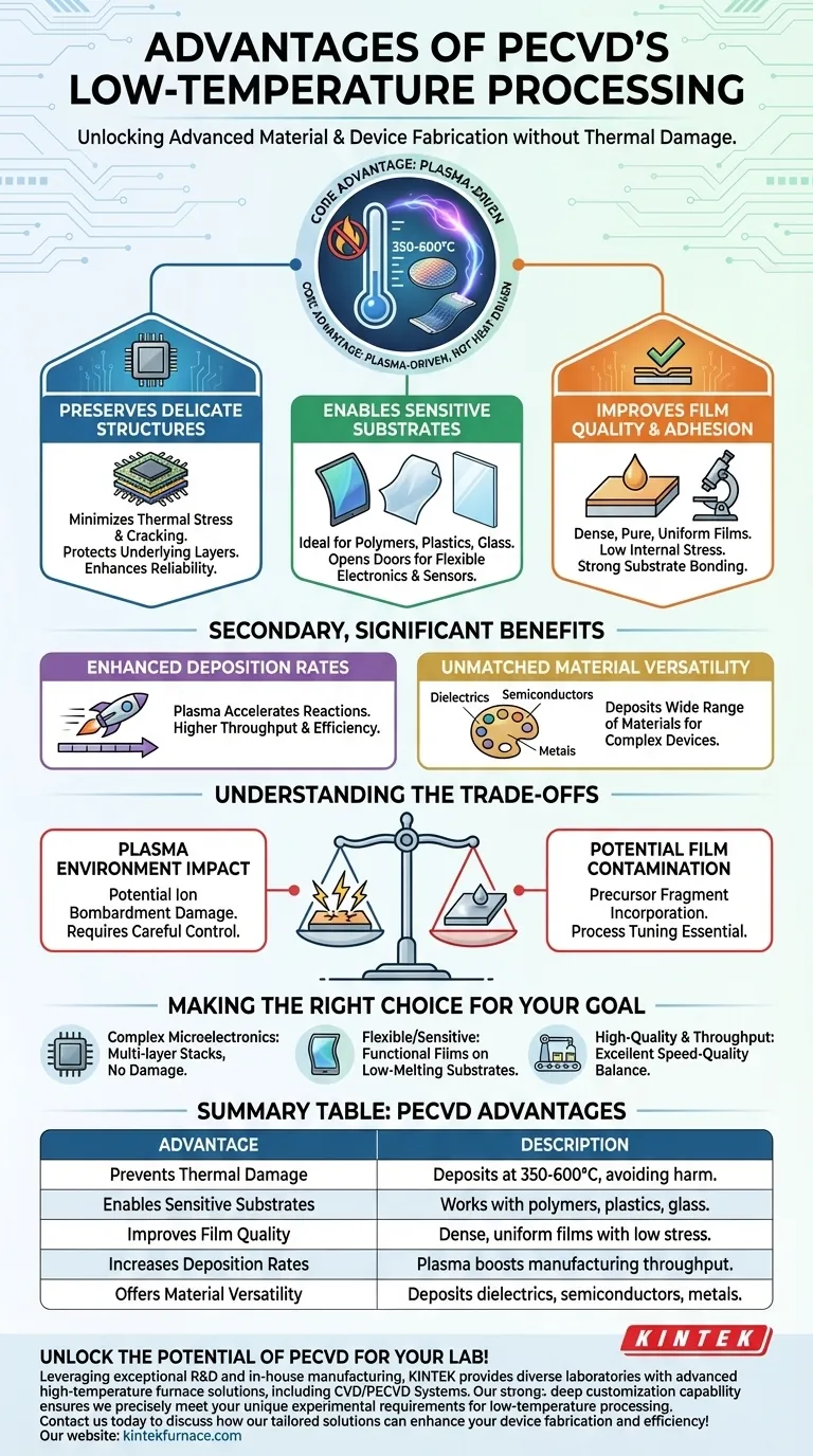
In short, the primary advantage of PECVD's low-temperature processing is its ability to deposit high-quality thin films without causing thermal damage. This capability is critical for building modern electronic devices that rely on complex, multi-layered structures and temperature-sensitive materials. By using plasma instead of high heat to drive chemical reactions, PECVD preserves the integrity of the underlying components.
The core value of low-temperature PECVD is not just a minor improvement; it fundamentally expands the universe of what can be manufactured. It allows for the creation of advanced devices on sensitive substrates that would be destroyed by the high temperatures of conventional deposition methods.
Why Low Temperature Is a Game-Changer
Traditional Chemical Vapor Deposition (CVD) relies on high temperatures (often >600°C) to provide the energy needed for chemical reactions. While effective, this thermal energy is indiscriminate and creates significant challenges. PECVD overcomes these by using an energy source—plasma—that is not based on heat.
Preserving Delicate Device Structures
In semiconductor manufacturing, devices are built layer by layer. Each new layer cannot damage the ones already present.
High temperatures cause thermal stress, as different materials expand and contract at different rates. This leads to cracking, delamination, and a loss of structural integrity, ultimately causing device failure.
PECVD operates at much lower temperatures (typically 350-600°C), minimizing this stress and preserving the intricate, pre-existing structures on a wafer. This directly enhances device performance and reliability.
Enabling a Wider Range of Substrates
Many promising technologies, like flexible electronics or advanced sensors, cannot be built on traditional silicon wafers. They require substrates that cannot withstand high heat.
PECVD's low-temperature capability makes it ideal for depositing films on temperature-sensitive materials such as polymers, plastics, and certain types of glass. This opens up applications that are impossible with high-temperature processes.
Improving Film Quality and Adhesion
One might assume lower temperature means lower quality, but PECVD defies this. The energy to drive the deposition reaction comes from the highly reactive species in the plasma, not just heat.
This plasma-driven process allows for the growth of films that are dense, pure, and uniform. The resulting films exhibit low internal stress and excellent adhesion to the substrate because they are not formed under the duress of extreme thermal expansion and contraction.
The Secondary, but Significant, Benefits
Beyond preventing thermal damage, the plasma-centric nature of PECVD provides other powerful advantages.
Enhanced Deposition Rates
The high-energy electrons within the plasma dramatically accelerate the chemical reactions required for film deposition.
This allows PECVD to achieve high deposition rates even at low temperatures, leading to greater manufacturing throughput and efficiency compared to many conventional thermal methods.
Unmatched Material Versatility
Because the process is not limited by the thermal stability of the substrate, PECVD can be used to deposit an exceptionally wide range of materials.
This includes dielectrics (like silicon nitride and silicon dioxide), semiconductors, and even metals. This versatility makes it a cornerstone technology for fabricating complex, multi-material devices.
Understanding the Trade-offs
While powerful, PECVD is not without its complexities. The introduction of plasma, while solving the heat problem, creates its own set of variables to manage.
The Impact of the Plasma Environment
The high-energy ions in the plasma can, if not properly controlled, cause physical damage to the substrate or film through ion bombardment. This can create defects that affect electrical performance.
Potential for Film Contamination
The chemical reactions in PECVD are complex. It is possible for precursor fragments, such as hydrogen, to become incorporated into the growing film. This can alter the film's desired electrical or optical properties. Careful process tuning is required to minimize these effects.
Making the Right Choice for Your Goal
Selecting PECVD is a strategic decision based on your specific material and device requirements.
- If your primary focus is complex microelectronics: PECVD is essential to deposit films in a multi-layer stack without damaging the underlying integrated circuits.
- If your primary focus is flexible electronics or sensitive materials: PECVD is the default choice for depositing functional films on polymers, plastics, or other low-melting-point substrates.
- If your primary focus is high-quality films at high throughput: PECVD provides an excellent balance of speed and quality, especially for depositing thick coatings or covering large areas uniformly.
Ultimately, PECVD's low-temperature capability is what unlocks the fabrication of today's most advanced materials and electronic devices.
Summary Table:
| Advantage | Description |
|---|---|
| Prevents Thermal Damage | Deposits films at 350-600°C, avoiding harm to delicate structures and materials. |
| Enables Sensitive Substrates | Works with polymers, plastics, and glass, expanding application possibilities. |
| Improves Film Quality | Plasma-driven process ensures dense, uniform films with low stress and strong adhesion. |
| Increases Deposition Rates | High-energy plasma accelerates reactions, boosting manufacturing throughput. |
| Offers Material Versatility | Deposits dielectrics, semiconductors, and metals for diverse device fabrication. |
Unlock the potential of PECVD for your lab! Leveraging exceptional R&D and in-house manufacturing, KINTEK provides diverse laboratories with advanced high-temperature furnace solutions, including CVD/PECVD Systems. Our strong deep customization capability ensures we precisely meet your unique experimental requirements for low-temperature processing. Contact us today to discuss how our tailored solutions can enhance your device fabrication and efficiency!
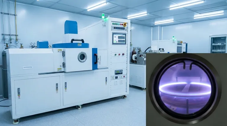
Visual Guide
Related Products
- Slide PECVD Tube Furnace with Liquid Gasifier PECVD Machine
- RF PECVD System Radio Frequency Plasma Enhanced Chemical Vapor Deposition
- Inclined Rotary Plasma Enhanced Chemical Deposition PECVD Tube Furnace Machine
- Inclined Rotary Plasma Enhanced Chemical Deposition PECVD Tube Furnace Machine
- Multi Heating Zones CVD Tube Furnace Machine for Chemical Vapor Deposition Equipment
People Also Ask
- What are the advantages of using a tube furnace CVD system for Cu(111)/graphene? Superior Scalability and Quality
- What role does a Tube Furnace play in the CVD growth of carbon nanotubes? Achieve High-Purity CNT Synthesis
- What is plasma in the context of PECVD? Unlock Low-Temperature Thin Film Deposition
- How does PECVD equipment contribute to TOPCon bottom cells? Mastering Hydrogenation for Maximum Solar Efficiency
- What are the main advantages of PECVD tube furnaces compared to CVD tube furnaces? Lower Temp, Faster Deposition, and More


