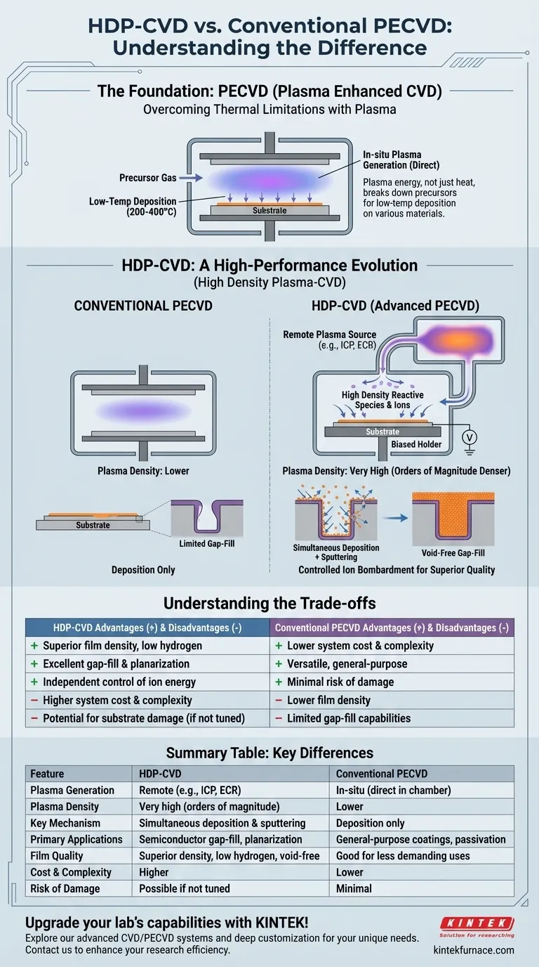
In essence, High Density Plasma Chemical Vapor Deposition (HDP-CVD) is an advanced form of Plasma Enhanced Chemical Vapor Deposition (PECVD) that utilizes a highly concentrated, remotely generated plasma. Unlike conventional PECVD, where the plasma is typically created directly within the reaction chamber, HDP-CVD decouples plasma generation from the substrate. This separation provides independent control over the density of reactive species and the energy of ions bombarding the film, enabling unique and superior film properties.
The fundamental difference is one of control and intent. While all PECVD methods use plasma to deposit films at low temperatures, HDP-CVD is specifically engineered to create a much denser plasma that enables simultaneous deposition and sputtering, leading to superior film quality and gap-fill capabilities for demanding applications.
The Foundation: Understanding PECVD
To grasp the significance of HDP-CVD, we must first understand the principle behind all PECVD processes.
Overcoming Thermal Limitations
Traditional Chemical Vapor Deposition (CVD) relies on high temperatures to provide the thermal energy needed to break down precursor gases and drive chemical reactions on a substrate surface. This works well for robust materials but is unsuitable for temperature-sensitive substrates like plastics or complex semiconductor devices.
The Role of Plasma
PECVD overcomes this limitation by introducing energy in the form of plasma. Instead of relying solely on heat, energetic electrons within the plasma collide with and break apart the precursor gas molecules. This creates a high concentration of reactive chemical species at much lower temperatures (typically 200-400°C), allowing for high-quality film deposition on a wider variety of materials.
HDP-CVD: A High-Performance Evolution
HDP-CVD is not just an incremental improvement; it is a specialized evolution of PECVD designed for applications where film density and conformal coverage are critical.
Decoupling Plasma Generation
In a conventional PECVD system, the plasma is generated "in-situ," meaning directly between the electrodes where the substrate sits. In an HDP-CVD system, the plasma is generated remotely in a separate chamber, often using an Inductively Coupled Plasma (ICP) or Electron Cyclotron Resonance (ECR) source.
This dense plasma of reactive species and ions is then directed toward the substrate in the main chamber.
Achieving Uniquely High Plasma Density
The remote sources used in HDP-CVD are capable of generating a plasma that is orders of magnitude denser than in conventional PECVD. This high density of reactive species dramatically increases the efficiency of the deposition process.
The Deposition + Sputtering Mechanism
The most critical feature of HDP-CVD is the ability to apply an independent electrical bias to the substrate holder. This bias attracts the high concentration of ions from the plasma, causing them to bombard the substrate with controlled energy.
This controlled ion bombardment results in a simultaneous process of deposition (from the reactive neutrals) and sputtering (physical etching by the ions). This sputtering effect preferentially removes loosely deposited material from sharp corners, allowing for exceptionally dense, void-free filling of high-aspect-ratio gaps, such as trenches in semiconductor manufacturing.
Understanding the Trade-offs
Choosing HDP-CVD involves evaluating its powerful advantages against its inherent complexities.
Film Quality vs. Process Cost
HDP-CVD produces films with superior density, lower hydrogen content, and excellent gap-fill capabilities. However, the systems are significantly more complex and expensive than conventional PECVD reactors, both to purchase and to maintain.
Application Specificity vs. Generality
Because of its unique deposition/sputtering mechanism, HDP-CVD is the go-to process for demanding semiconductor gap-fill and planarization. Conventional PECVD is a more versatile, general-purpose tool suitable for a broader range of applications, such as passivation layers or simple coatings where gap-fill is not a concern.
Controlled Bombardment vs. Potential Damage
While HDP-CVD offers precise control over ion energy, the process is inherently based on ion bombardment. If not tuned correctly, this can induce damage in sensitive underlying device layers. Other remote PECVD techniques exist that use ion screening to ensure only neutral species reach the substrate, offering the lowest-damage process possible at the expense of HDP's gap-fill benefits.
Making the Right Choice for Your Goal
Your decision must be driven by the specific requirements of the film you need to create.
- If your primary focus is depositing high-quality, dense, and void-free films for advanced applications like semiconductor gap-fill: HDP-CVD is the superior choice due to its controlled ion bombardment and high-density plasma.
- If your primary focus is general-purpose film deposition, such as passivation layers on less complex or temperature-sensitive substrates where cost and throughput are key factors: Conventional PECVD offers a simpler, more cost-effective, and robust solution.
- If your primary focus is depositing a film with minimal to zero ion bombardment on an extremely sensitive electronic or optical device: A remote PECVD system specifically designed with ion screening would be the most appropriate method.
Ultimately, the choice between HDP-CVD and other PECVD methods hinges on a clear understanding of your required film properties and application demands.
Summary Table:
| Feature | HDP-CVD | Conventional PECVD |
|---|---|---|
| Plasma Generation | Remote (e.g., ICP, ECR) | In-situ (direct in chamber) |
| Plasma Density | Very high (orders of magnitude denser) | Lower |
| Key Mechanism | Simultaneous deposition and sputtering | Deposition only |
| Primary Applications | Semiconductor gap-fill, planarization | General-purpose coatings, passivation layers |
| Film Quality | Superior density, low hydrogen, void-free | Good for less demanding uses |
| Cost and Complexity | Higher | Lower |
| Risk of Substrate Damage | Possible if not tuned | Minimal |
Upgrade your lab's capabilities with KINTEK's advanced high-temperature furnace solutions! Leveraging exceptional R&D and in-house manufacturing, we provide diverse laboratories with cutting-edge products like CVD/PECVD Systems, Muffle, Tube, Rotary Furnaces, and Vacuum & Atmosphere Furnaces. Our strong deep customization capability ensures we precisely meet your unique experimental needs, such as optimizing HDP-CVD processes for superior semiconductor applications. Contact us today to discuss how we can enhance your research and production efficiency!
Visual Guide
Related Products
- HFCVD Machine System Equipment for Drawing Die Nano Diamond Coating
- Multi Heating Zones CVD Tube Furnace Machine for Chemical Vapor Deposition Equipment
- Controlled Inert Nitrogen Hydrogen Atmosphere Furnace
- Split Chamber CVD Tube Furnace with Vacuum Station CVD Machine
- Custom Made Versatile CVD Tube Furnace Chemical Vapor Deposition CVD Equipment Machine
People Also Ask
- What role does Chemical Vapor Deposition (CVD) equipment play in the surface coating of carbon fibers for composites?
- What is Hot-filament Chemical Vapor Deposition (HFCVD)? Achieve High-Quality Thin Films with Precision Control
- What is chemical vapor deposition (CVD) and its primary industrial application? Unlock Precision Thin Films for Electronics
- What materials are commonly used in CVD coating systems? Explore Key Materials for Superior Coatings
- What core function does CVD equipment serve in h-BN anti-corrosion? Master Precision Synthesis for High-Performance Films