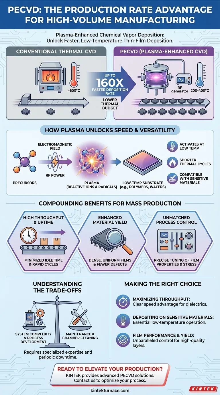
At its core, the primary production advantage of Plasma-Enhanced Chemical Vapor Deposition (PECVD) is its ability to deposit high-quality thin films at a significantly faster rate than conventional methods. This acceleration is achieved by using an energy-rich plasma to drive chemical reactions at much lower temperatures. For example, depositing silicon nitride can be up to 160 times faster with PECVD compared to traditional Chemical Vapor Deposition (CVD), enabling a dramatic increase in manufacturing throughput.
The true advantage of PECVD in a production environment is not just its speed, but its ability to combine that speed with low temperatures. This combination unlocks high-yield, cost-effective mass production for a wider range of materials and complex devices that cannot tolerate high heat.
How Plasma Unlocks High-Speed Production
The fundamental difference between PECVD and conventional thermal CVD is its energy source. This distinction is the key to its production efficiency.
Activating Precursors at Low Temperatures
In traditional CVD, high temperatures (often >600°C) are required to provide enough thermal energy to break down the precursor gases and initiate the chemical reaction on the substrate surface.
PECVD replaces the need for intense heat with an electromagnetic field (typically Radio Frequency, or RF). This field energizes the process gases into a plasma, a state of matter containing highly reactive ions and radicals.
These reactive species can then deposit onto the substrate and form a high-quality film at much lower temperatures (typically 200-400°C).
The Production Impact of Lower Temperatures
Operating at lower temperatures directly translates to faster production cycles. Substrates do not need to be slowly heated to extreme temperatures and then cooled down.
This shortened thermal budget not only increases units per hour but also makes PECVD compatible with temperature-sensitive materials, such as polymers or semiconductor wafers with previously fabricated layers, expanding its manufacturing applications.
The Compounding Benefits for Mass Production
The high deposition rate is just the beginning. Several other factors make PECVD a superior choice for high-volume manufacturing environments like solar cell or semiconductor fabrication.
High Throughput and Uptime
Modern PECVD systems are often modular and designed for continuous operation. The combination of rapid deposition, direct substrate heating, and showerhead gas inlets leads to uniform films created in short cycles.
This focus on efficiency minimizes idle time. Furthermore, systems are designed for high uptime with minimal interruptions for maintenance and cleaning, maximizing the output of a production line.
Enhanced Material Yield
Production rate is meaningless if the products are defective. PECVD excels at producing films that are dense, uniform, and have excellent adhesion.
This results in fewer pinholes and a reduced risk of cracking compared to other methods. Higher quality means fewer rejected parts, which directly improves material yield and lowers the effective cost per unit.
Unmatched Process Control
The plasma process offers multiple levers for control. By adjusting parameters like RF power, frequency, pressure, and gas composition, engineers can precisely tune the final properties of the film.
This allows for fine control over film stress, stoichiometry, and density. In production, this means a single machine can be configured to produce films with different characteristics, adding versatility and value to the manufacturing line. A key example is creating hydrogen-rich silicon nitride films for solar cells to passivate defects and boost efficiency.
Understanding the Trade-offs
While powerful, PECVD is not a universal solution. Acknowledging its complexities is key to a successful implementation.
System Complexity
A PECVD system is more complex than a simple thermal CVD reactor. It involves a vacuum chamber, high-power RF generators, and sophisticated gas handling systems. This equipment requires specialized knowledge to operate and maintain.
Process Development
The high degree of control is also a source of complexity. Developing a stable, repeatable process recipe requires significant expertise and experimentation to optimize the many interdependent parameters for a specific film and application.
Maintenance and Chamber Cleaning
Although often designed for easier maintenance, the inside of the chamber will eventually get coated with deposited material. This requires periodic downtime for cleaning to prevent particle contamination on subsequent production runs. This downtime must be factored into any throughput calculation.
Making the Right Choice for Your Goal
To determine if PECVD is the right fit, align its capabilities with your primary production objective.
- If your primary focus is maximizing throughput: PECVD's rapid deposition rates offer a clear and significant speed advantage over conventional thermal CVD for many dielectric materials.
- If your primary focus is depositing on sensitive materials: The low-temperature operation is the most critical feature, enabling high-quality film growth on substrates that cannot withstand high heat.
- If your primary focus is film performance and yield: PECVD provides unparalleled control over film properties, allowing you to engineer functional layers with high uniformity and adhesion, leading to fewer defects and higher overall yield.
Ultimately, choosing PECVD is a strategic decision to prioritize a combination of speed, quality, and material versatility in a production environment.
Summary Table:
| Advantage | Key Benefit | Impact on Production |
|---|---|---|
| High Deposition Rate | Up to 160x faster than CVD | Increases throughput and units per hour |
| Low-Temperature Operation | Works at 200-400°C | Enables use with sensitive materials, reduces thermal cycles |
| Enhanced Film Quality | Dense, uniform films with excellent adhesion | Improves material yield and reduces defects |
| Superior Process Control | Tunable film properties via RF power, pressure, etc. | Allows versatile production and high repeatability |
| High Uptime and Modularity | Designed for continuous operation with minimal downtime | Maximizes production line efficiency and output |
Ready to elevate your production with advanced PECVD solutions? Leveraging exceptional R&D and in-house manufacturing, KINTEK provides diverse laboratories with high-temperature furnace solutions, including our specialized CVD/PECVD Systems. Our strong deep customization capability ensures we precisely meet your unique experimental requirements for faster, higher-yield thin-film deposition. Contact us today to discuss how our tailored PECVD systems can optimize your manufacturing processes and drive innovation in your lab!
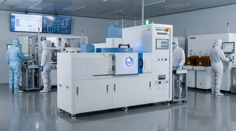
Visual Guide
Related Products
- Slide PECVD Tube Furnace with Liquid Gasifier PECVD Machine
- RF PECVD System Radio Frequency Plasma Enhanced Chemical Vapor Deposition
- Inclined Rotary Plasma Enhanced Chemical Deposition PECVD Tube Furnace Machine
- Inclined Rotary Plasma Enhanced Chemical Deposition PECVD Tube Furnace Machine
- Multi Heating Zones CVD Tube Furnace Machine for Chemical Vapor Deposition Equipment
People Also Ask
- What are the advantages of using a tube furnace CVD system for Cu(111)/graphene? Superior Scalability and Quality
- What role does a Tube Furnace play in the CVD growth of carbon nanotubes? Achieve High-Purity CNT Synthesis
- How does PECVD equipment contribute to TOPCon bottom cells? Mastering Hydrogenation for Maximum Solar Efficiency
- What are the typical conditions for plasma-enhanced CVD processes? Achieve Low-Temperature Thin Film Deposition
- What is plasma in the context of PECVD? Unlock Low-Temperature Thin Film Deposition


