PECVD contributes to the formation of (n)poly-Si layers by utilizing plasma energy to decompose specific precursor gases—Silane (SiH4), Hydrogen (H2), and Phosphine (PH3)—at relatively low temperatures. Instead of directly depositing polycrystalline silicon, the system deposits a layer of in-situ doped amorphous silicon (a-Si), which serves as the structural and chemical foundation that is subsequently transformed into the final (n)poly-Si film.
The core value of PECVD in this application is its ability to achieve uniform phosphorus distribution within the film while maintaining high production throughput, establishing the essential baseline for high-quality passivating contacts.
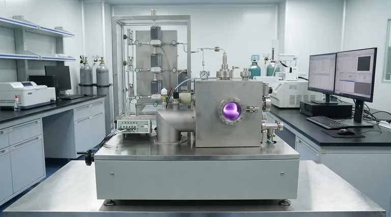
The Mechanism of Deposition
Plasma-Driven Decomposition
The primary function of the PECVD system is to generate energy without relying solely on heat.
By applying a high-frequency electric field, the system initiates a glow discharge, creating a plasma that ionizes the gas mixture. This allows for the decomposition of Silane (SiH4) and Phosphine (PH3) at substrate temperatures significantly lower than those required for conventional thermal CVD.
In-Situ Doping
A critical contribution of the PECVD process is the ability to dope the material during deposition (in-situ).
By introducing Phosphine (PH3) alongside Silane, phosphorus atoms are incorporated directly into the growing lattice. This ensures a uniform distribution of phosphorus throughout the thin film, which is essential for the electrical performance of (n)-type layers.
Surface Reaction and Film Growth
Once the plasma generates reactive species (ions, radicals, and electrons), these species diffuse to the substrate surface.
They engage in chemical reactions to form a solid film on top of the target surface (often an SiOx layer). The system allows for precise control over the film thickness, ranging from nanometers to millimeters, depending on the duration and process parameters.
The Role in Passivating Contacts
Establishing the Foundation
The primary reference highlights that the PECVD process deposits in-situ doped amorphous silicon (a-Si).
While the user's goal is (n)poly-Si, the PECVD step provides the necessary precursor: a doped amorphous layer deposited onto SiOx. This stack is the "foundation" that enables the creation of high-quality passivating contacts, typically crystallized into poly-Si in subsequent processing steps.
High-Throughput Manufacturing
PECVD is specifically noted for its high-throughput production capabilities.
The kinetic energy supplied by the plasma accelerates the chemical reactions, making the deposition rate faster than many standard thermal processes. This speed is vital for industrial scaling of semiconductor and solar cell components.
Operational Considerations and Trade-offs
Parameter Sensitivity
While PECVD offers speed and low-temperature operation, it introduces complexity in process control.
The quality of the deposited film is highly dependent on a specific balance of gas flow rates, chamber pressure, and plasma power. Variations in these parameters can alter the film's properties, requiring strict monitoring to ensure reproducibility.
By-product Management
The chemical reactions driven by the plasma generate volatile by-products.
To maintain film purity, the system must effectively continuously remove these by-products via diffusion and convection. Failure to manage this exhaust can lead to contamination of the deposited layer.
Making the Right Choice for Your Goal
How to Apply This to Your Project
- If your primary focus is Scalability: Leverage PECVD for its high-throughput capabilities to deposit precursor layers rapidly across large volumes.
- If your primary focus is Electrical Performance: Rely on the system's ability to achieve uniform in-situ doping of phosphorus to ensure consistent conductivity in your passivating contacts.
- If your primary focus is Substrate Integrity: Utilize the low-temperature nature of the plasma process to coat sensitive substrates that cannot withstand the high heat of thermal CVD.
PECVD provides the critical balance of speed, doping uniformity, and thermal management required to build the foundation of modern conductive layers.
Summary Table:
| Feature | PECVD Contribution to (n)poly-Si | Benefit for Manufacturing |
|---|---|---|
| Energy Source | High-frequency plasma (glow discharge) | Enables deposition at lower substrate temperatures |
| Doping Method | In-situ Phosphine (PH3) introduction | Ensures uniform phosphorus distribution and conductivity |
| Precursor Form | Deposits doped amorphous silicon (a-Si) | Provides the essential foundation for passivating contacts |
| Growth Rate | Accelerated chemical reaction kinetics | High-throughput production for industrial scaling |
| Process Control | Gas flow, pressure, and power modulation | High precision in film thickness and material purity |
Maximize Your Deposition Precision with KINTEK
Are you looking to scale your semiconductor or solar cell production? KINTEK provides industry-leading CVD and PECVD systems specifically engineered for high-throughput manufacturing and uniform in-situ doping.
Backed by expert R&D and manufacturing, our systems—including Muffle, Tube, Rotary, Vacuum, and CVD systems—are fully customizable to meet your unique thin-film requirements. Let our expertise in high-temperature lab equipment help you achieve superior electrical performance and substrate integrity.
Ready to optimize your (n)poly-Si process? Contact us today to discuss your custom solution!
References
- TiN <sub> <i>x</i> </sub> and TiO <sub> <i>x</i> </sub> /TiN <sub> <i>x</i> </sub> Barrier Layers for Al‐Based Metallization of Passivating Contacts in Si Solar Cells. DOI: 10.1002/pssr.202500168
This article is also based on technical information from Kintek Furnace Knowledge Base .
Related Products
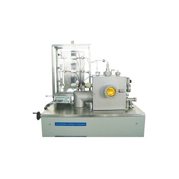
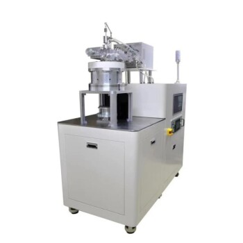
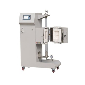
- Inclined Rotary Plasma Enhanced Chemical Deposition PECVD Tube Furnace Machine
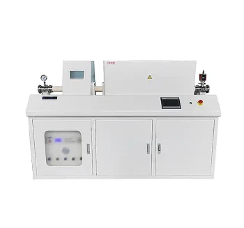
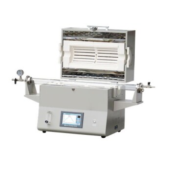
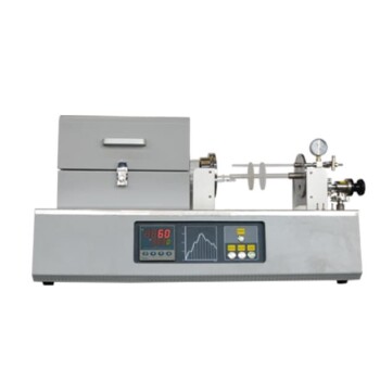
- Slide PECVD Tube Furnace with Liquid Gasifier PECVD Machine
- Inclined Rotary Plasma Enhanced Chemical Deposition PECVD Tube Furnace Machine
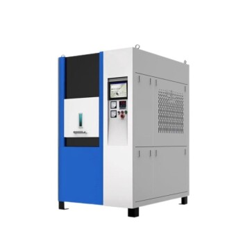
- RF PECVD System Radio Frequency Plasma Enhanced Chemical Vapor Deposition
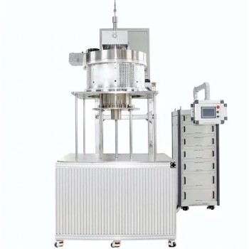
- MPCVD Machine System Reactor Bell-jar Resonator for Lab and Diamond Growth
People Also Ask
- What are the future trends in CVD technology? AI, Sustainability, and Advanced Materials
- What methods are used to analyze and characterize graphene samples? Unlock Key Techniques for Accurate Material Analysis
- Why Use PECVD for Monolithic Integrated Chip Isolation Layers? Protect Your Thermal Budget with High-Quality SiO2
- What advantages does the Laser Chemical Vapor Deposition (LCVD) process offer? High Purity & Precision SiC Fibers
- What are the technical advantages of using a CVD system? Optimize Carbon Nanotube Growth for Thermal Conductivity
